P89V51RB2BBC,557 NXP Semiconductors, P89V51RB2BBC,557 Datasheet - Page 9
P89V51RB2BBC,557
Manufacturer Part Number
P89V51RB2BBC,557
Description
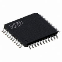
IC 80C51 MCU 1024 RAM 44TQFP
Manufacturer
NXP Semiconductors
Series
89Vr
Datasheet
1.P89V51RC2FBC557.pdf
(80 pages)
Specifications of P89V51RB2BBC,557
Program Memory Type
FLASH
Program Memory Size
16KB (16K x 8)
Package / Case
44-TQFP, 44-VQFP
Core Processor
8051
Core Size
8-Bit
Speed
40MHz
Connectivity
SPI, UART/USART
Peripherals
Brown-out Detect/Reset, POR, PWM, WDT
Number Of I /o
32
Ram Size
1K x 8
Voltage - Supply (vcc/vdd)
4.5 V ~ 5.5 V
Oscillator Type
Internal
Operating Temperature
0°C ~ 70°C
Processor Series
P89V5x
Core
80C51
Data Bus Width
8 bit
Data Ram Size
1 KB
Interface Type
SPI, UART
Maximum Clock Frequency
40 MHz
Number Of Programmable I/os
32
Number Of Timers
3
Maximum Operating Temperature
+ 70 C
Mounting Style
SMD/SMT
3rd Party Development Tools
PK51, CA51, A51, ULINK2
Minimum Operating Temperature
0 C
Lead Free Status / RoHS Status
Lead free / RoHS Compliant
For Use With
622-1017 - BOARD 44-ZIF PLCC SOCKET
Eeprom Size
-
Data Converters
-
Lead Free Status / Rohs Status
Lead free / RoHS Compliant
Other names
935277723557
P89V51RB2BBC
P89V51RB2BBC
P89V51RB2BBC
P89V51RB2BBC
Available stocks
Company
Part Number
Manufacturer
Quantity
Price
Company:

Part Number:
P89V51RB2BBC,557
Manufacturer:
NXP Semiconductors
Quantity:
10 000


NXP Semiconductors
Table 3.
[1]
[2]
P89V51RB2_RC2_RD2_5
Product data sheet
Symbol
RST
EA
ALE/PROG
n.c.
XTAL1
XTAL2
V
V
DD
SS
ALE loading issue: When ALE pin experiences higher loading (>30 pF) during the reset, the microcontroller may accidentally enter into
modes other than normal working mode. The solution is to add a pull-up resistor of 3 k to 50 k to V
For 6-clock mode, ALE is emitted at
P89V51RB2/RC2/RD2 pin description
Pin
DIP40
9
31
30
-
19
18
40
20
TQFP44
4
29
27
6, 17, 28,
39
15
14
38
16
1
3
of crystal frequency.
PLCC44
10
35
33
1, 12, 23,
34
21
20
44
22
Rev. 05 — 12 November 2009
…continued
Type
I
I
I/O
I/O
I
O
I
I
Description
Reset: While the oscillator is running, a HIGH logic state
on this pin for two machine cycles will reset the device. If
the PSEN pin is driven by a HIGH-to-LOW input transition
while the RST input pin is held HIGH, the device will enter
the external host mode, otherwise the device will enter the
normal operation mode.
External Access Enable: EA must be connected to V
order to enable the device to fetch code from the external
program memory. EA must be strapped to V
program execution. The EA pin can tolerate a high voltage
of 12 V.
Address Latch Enable: ALE is the output signal for
latching the low byte of the address during an access to
external memory. This pin is also the programming pulse
input (PROG) for flash programming. Normally the ALE
is emitted at a constant rate of
and can be used for external timing and clocking. One ALE
pulse is skipped during each access to external data
memory. However, if AO is set to ‘1’, ALE is disabled.
not connected
Crystal 1: Input to the inverting oscillator amplifier and
input to the internal clock generator circuits.
Crystal 2: Output from the inverting oscillator amplifier.
Power supply
Ground
P89V51RB2/RC2/RD2
8-bit microcontrollers with 80C51 core
DD
1
, e.g., for ALE pin.
6
the crystal frequency
© NXP B.V. 2009. All rights reserved.
DD
for internal
9 of 80
SS
[2]
[1]
in
Related parts for P89V51RB2BBC,557
Image
Part Number
Description
Manufacturer
Datasheet
Request
R

Part Number:
Description:
8-bit 80c51 5 V Low Power 16/32/64 Kb Flash Microcontroller With 1 Kb Ram
Manufacturer:
NXP Semiconductors
Datasheet:
Part Number:
Description:
NXP Semiconductors designed the LPC2420/2460 microcontroller around a 16-bit/32-bitARM7TDMI-S CPU core with real-time debug interfaces that include both JTAG andembedded trace
Manufacturer:
NXP Semiconductors
Datasheet:

Part Number:
Description:
NXP Semiconductors designed the LPC2458 microcontroller around a 16-bit/32-bitARM7TDMI-S CPU core with real-time debug interfaces that include both JTAG andembedded trace
Manufacturer:
NXP Semiconductors
Datasheet:
Part Number:
Description:
NXP Semiconductors designed the LPC2468 microcontroller around a 16-bit/32-bitARM7TDMI-S CPU core with real-time debug interfaces that include both JTAG andembedded trace
Manufacturer:
NXP Semiconductors
Datasheet:
Part Number:
Description:
NXP Semiconductors designed the LPC2470 microcontroller, powered by theARM7TDMI-S core, to be a highly integrated microcontroller for a wide range ofapplications that require advanced communications and high quality graphic displays
Manufacturer:
NXP Semiconductors
Datasheet:
Part Number:
Description:
NXP Semiconductors designed the LPC2478 microcontroller, powered by theARM7TDMI-S core, to be a highly integrated microcontroller for a wide range ofapplications that require advanced communications and high quality graphic displays
Manufacturer:
NXP Semiconductors
Datasheet:
Part Number:
Description:
The Philips Semiconductors XA (eXtended Architecture) family of 16-bit single-chip microcontrollers is powerful enough to easily handle the requirements of high performance embedded applications, yet inexpensive enough to compete in the market for hi
Manufacturer:
NXP Semiconductors
Datasheet:
Part Number:
Description:
The XA-S3 device is a member of Philips Semiconductors? XA(eXtended Architecture) family of high performance 16-bitsingle-chip microcontrollers
Manufacturer:
NXP Semiconductors
Datasheet:

Part Number:
Description:
The NXP BlueStreak LH75401/LH75411 family consists of two low-cost 16/32-bit System-on-Chip (SoC) devices
Manufacturer:
NXP Semiconductors
Datasheet:
Part Number:
Description:
The NXP LPC3130/3131 combine an 180 MHz ARM926EJ-S CPU core, high-speed USB2
Manufacturer:
NXP Semiconductors
Datasheet:
Part Number:
Description:
The NXP LPC3141 combine a 270 MHz ARM926EJ-S CPU core, High-speed USB 2
Manufacturer:
NXP Semiconductors
Part Number:
Description:
The NXP LPC3143 combine a 270 MHz ARM926EJ-S CPU core, High-speed USB 2
Manufacturer:
NXP Semiconductors

Part Number:
Description:
The NXP LPC3152 combines an 180 MHz ARM926EJ-S CPU core, High-speed USB 2
Manufacturer:
NXP Semiconductors
Part Number:
Description:
The NXP LPC3154 combines an 180 MHz ARM926EJ-S CPU core, High-speed USB 2
Manufacturer:
NXP Semiconductors