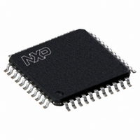
P89V51RB2BBC,557 NXP Semiconductors, P89V51RB2BBC,557 Datasheet - Page 7

P89V51RB2BBC,557
Manufacturer Part Number
P89V51RB2BBC,557
Description
IC 80C51 MCU 1024 RAM 44TQFP
Manufacturer
NXP Semiconductors
Series
89Vr
Datasheet
1.P89V51RC2FBC557.pdf
(80 pages)
Specifications of P89V51RB2BBC,557
Program Memory Type
FLASH
Program Memory Size
16KB (16K x 8)
Package / Case
44-TQFP, 44-VQFP
Core Processor
8051
Core Size
8-Bit
Speed
40MHz
Connectivity
SPI, UART/USART
Peripherals
Brown-out Detect/Reset, POR, PWM, WDT
Number Of I /o
32
Ram Size
1K x 8
Voltage - Supply (vcc/vdd)
4.5 V ~ 5.5 V
Oscillator Type
Internal
Operating Temperature
0°C ~ 70°C
Processor Series
P89V5x
Core
80C51
Data Bus Width
8 bit
Data Ram Size
1 KB
Interface Type
SPI, UART
Maximum Clock Frequency
40 MHz
Number Of Programmable I/os
32
Number Of Timers
3
Maximum Operating Temperature
+ 70 C
Mounting Style
SMD/SMT
3rd Party Development Tools
PK51, CA51, A51, ULINK2
Minimum Operating Temperature
0 C
Lead Free Status / RoHS Status
Lead free / RoHS Compliant
For Use With
622-1017 - BOARD 44-ZIF PLCC SOCKET
Eeprom Size
-
Data Converters
-
Lead Free Status / Rohs Status
Lead free / RoHS Compliant
Other names
935277723557
P89V51RB2BBC
P89V51RB2BBC
P89V51RB2BBC
P89V51RB2BBC
Available stocks
Company
Part Number
Manufacturer
Quantity
Price
Company:
Part Number:
P89V51RB2BBC,557
Manufacturer:
NXP Semiconductors
Quantity:
10 000
NXP Semiconductors
Table 3.
P89V51RB2_RC2_RD2_5
Product data sheet
Symbol
P1.2/ECI
P1.3/CEX0
P1.4/SS/CEX1 5
P1.5/MOSI/
CEX2
P1.6/MISO/
CEX3
P1.7/SPICLK/
CEX4
P2.0 to P2.7
P2.0/A8
P2.1/A9
P2.2/A10
P2.3/A11
P2.4/A12
P89V51RB2/RC2/RD2 pin description
Pin
DIP40
3
4
6
7
8
21
22
23
24
25
TQFP44
42
43
44
1
2
3
18
19
20
21
22
PLCC44
4
5
6
7
8
9
24
25
26
27
28
Rev. 05 — 12 November 2009
…continued
Type
I/O
I
I/O
I/O
I/O
I
I/O
I/O
I/O
I/O
I/O
I/O
I/O
I/O
I/O
I/O
I/O with
internal
pull-up
I/O
O
I/O
O
I/O
O
I/O
O
I/O
O
Description
P1.2 — Port 1 bit 2.
ECI — External clock input. This signal is the external
clock input for the PCA.
P1.3 — Port 1 bit 3.
CEX0 — Capture/compare external I/O for PCA Module 0.
Each capture/compare module connects to a Port 1 pin for
external I/O. When not used by the PCA, this pin can
handle standard I/O.
P1.4 — Port 1 bit 4.
SS — Slave port select input for SPI.
CEX1 — Capture/compare external I/O for PCA Module 1.
P1.5 — Port 1 bit 5.
MOSI — Master Output Slave Input for SPI.
CEX2 — Capture/compare external I/O for PCA Module 2.
P1.6 — Port 1 bit 6.
MISO — Master Input Slave Output for SPI.
CEX3 — Capture/compare external I/O for PCA Module 3.
P1.7 — Port 1 bit 7.
SPICLK — Serial clock input/output for SPI.
CEX4 — Capture/compare external I/O for PCA Module 4.
Port 2: Port 2 is an 8-bit bidirectional I/O port with internal
pull-ups. Port 2 pins are pulled HIGH by the internal
pull-ups when ‘1’s are written to them and can be used as
inputs in this state. As inputs, Port 2 pins that are
externally pulled LOW will source current (I
the internal pull-ups. Port 2 sends the high-order address
byte during fetches from external program memory and
during accesses to external Data Memory that use 16-bit
address (MOVX@DPTR). In this application, it uses strong
internal pull-ups when transitioning to ‘1’s. Port 2 also
receives some control signals and a partial of high-order
address bits during the external host mode programming
and verification.
P2.0 — Port 2 bit 0.
A8 — Address bit 8.
P2.1 — Port 2 bit 1.
A9 — Address bit 9.
P2.2 — Port 2 bit 2.
A10 — Address bit 10.
P2.3 — Port 2 bit 3.
A11 — Address bit 11.
P2.4 — Port 2 bit 4.
A12 — Address bit 12.
P89V51RB2/RC2/RD2
8-bit microcontrollers with 80C51 core
© NXP B.V. 2009. All rights reserved.
IL
) because of
7 of 80


