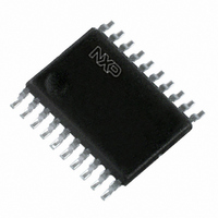
P89LPC922A1FDH,112 NXP Semiconductors, P89LPC922A1FDH,112 Datasheet - Page 43

P89LPC922A1FDH,112
Manufacturer Part Number
P89LPC922A1FDH,112
Description
IC 80C51 MCU FLASH 8K 20-TSSOP
Manufacturer
NXP Semiconductors
Series
LPC900r
Datasheet
1.P89LPC9201FDH112.pdf
(75 pages)
Specifications of P89LPC922A1FDH,112
Program Memory Type
FLASH
Program Memory Size
8KB (8K x 8)
Package / Case
20-TSSOP
Core Processor
8051
Core Size
8-Bit
Speed
18MHz
Connectivity
I²C, UART/USART
Peripherals
Brown-out Detect/Reset, POR, PWM, WDT
Number Of I /o
18
Ram Size
256 x 8
Voltage - Supply (vcc/vdd)
2.4 V ~ 3.6 V
Oscillator Type
Internal
Operating Temperature
-40°C ~ 85°C
Processor Series
P89LPC
Core
80C51
Data Bus Width
8 bit
Data Ram Size
256 B
Interface Type
I2C, SPI, UART
Maximum Clock Frequency
18 MHz
Number Of Programmable I/os
15
Number Of Timers
2
Operating Supply Voltage
2.4 V to 3.6 V
Maximum Operating Temperature
+ 85 C
Mounting Style
SMD/SMT
3rd Party Development Tools
PK51, CA51, A51, ULINK2
Minimum Operating Temperature
- 40 C
On-chip Adc
8 bit, 4 Channel
Lead Free Status / RoHS Status
Lead free / RoHS Compliant
Eeprom Size
-
Data Converters
-
Lead Free Status / Rohs Status
Lead free / RoHS Compliant
Other names
935288637112
NXP Semiconductors
P89LPC92X1
Product data sheet
Fig 14. Watchdog timer in Watchdog mode (WDTE = 1)
watchdog
oscillator
(1) Watchdog reset can also be caused by an invalid feed sequence, or by writing to WDCON not immediately followed by a feed
PCLK
sequence.
7.27.1 Software reset
7.27.2 Dual data pointers
7.28.1 General description
0
1
7.27 Additional features
7.28 Flash program memory
MOV WFEED1, #0A5H
MOV WFEED2, #05AH
oscillator
crystal
The SRST bit in AUXR1 gives software the opportunity to reset the processor completely,
as if an external reset or watchdog reset had occurred. Care should be taken when writing
to AUXR1 to avoid accidental software resets.
The dual Data Pointers (DPTR) provides two different Data Pointers to specify the
address used with certain instructions. The DPS bit in the AUXR1 register selects one of
the two Data Pointers. Bit 2 of AUXR1 is permanently wired as a logic 0 so that the DPS
bit may be toggled (thereby switching Data Pointers) simply by incrementing the AUXR1
register, without the possibility of inadvertently altering other bits in the register.
The P89LPC9201/9211/922A1/9241/9251 flash memory provides in-circuit electrical
erasure and programming. The flash can be erased, read, and written as bytes. The
Sector and Page Erase functions can erase any flash sector (1 kB) or page (64 bytes).
The Chip Erase operation will erase the entire program memory. ICP using standard
commercial programmers is available. In addition, IAP and byte-erase allows code
memory to be used for non-volatile data storage. On-chip erase and write timing
generation contribute to a user-friendly programming interface. The
P89LPC9201/9211/922A1/9241/9251 flash reliably stores memory contents even after
100,000 erase and program cycles. The cell is designed to optimize the erase and
XTALWD
0
1
WDCON (A7H)
÷32
All information provided in this document is subject to legal disclaimers.
PRE2
Rev. 2 — 1 December 2010
P89LPC9201/9211/922A1/9241/
PRESCALER
PRE1
PRE0
SHADOW REGISTER
-
8-bit microcontroller with 8-bit ADC
-
8-BIT DOWN
WDL (C1H)
COUNTER
WDRUN
WDTOF
© NXP B.V. 2010. All rights reserved.
WDCLK
002aae015
reset
43 of 75
(1)


