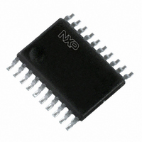
P89LPC922A1FDH,112 NXP Semiconductors, P89LPC922A1FDH,112 Datasheet - Page 37

P89LPC922A1FDH,112
Manufacturer Part Number
P89LPC922A1FDH,112
Description
IC 80C51 MCU FLASH 8K 20-TSSOP
Manufacturer
NXP Semiconductors
Series
LPC900r
Datasheet
1.P89LPC9201FDH112.pdf
(75 pages)
Specifications of P89LPC922A1FDH,112
Program Memory Type
FLASH
Program Memory Size
8KB (8K x 8)
Package / Case
20-TSSOP
Core Processor
8051
Core Size
8-Bit
Speed
18MHz
Connectivity
I²C, UART/USART
Peripherals
Brown-out Detect/Reset, POR, PWM, WDT
Number Of I /o
18
Ram Size
256 x 8
Voltage - Supply (vcc/vdd)
2.4 V ~ 3.6 V
Oscillator Type
Internal
Operating Temperature
-40°C ~ 85°C
Processor Series
P89LPC
Core
80C51
Data Bus Width
8 bit
Data Ram Size
256 B
Interface Type
I2C, SPI, UART
Maximum Clock Frequency
18 MHz
Number Of Programmable I/os
15
Number Of Timers
2
Operating Supply Voltage
2.4 V to 3.6 V
Maximum Operating Temperature
+ 85 C
Mounting Style
SMD/SMT
3rd Party Development Tools
PK51, CA51, A51, ULINK2
Minimum Operating Temperature
- 40 C
On-chip Adc
8 bit, 4 Channel
Lead Free Status / RoHS Status
Lead free / RoHS Compliant
Eeprom Size
-
Data Converters
-
Lead Free Status / Rohs Status
Lead free / RoHS Compliant
Other names
935288637112
NXP Semiconductors
P89LPC92X1
Product data sheet
7.20.6 Timer overflow toggle output
7.22.1 Mode 0
7.22.2 Mode 1
7.22.3 Mode 2
7.21 RTC/system timer
7.22 UART
Timers 0 and 1 can be configured to automatically toggle a port output whenever a timer
overflow occurs. The same device pins that are used for the T0 and T1 count inputs are
also used for the timer toggle outputs. The port outputs will be a logic 1 prior to the first
timer overflow when this mode is turned on.
The P89LPC9201/9211/922A1/9241/9251 has a simple RTC that allows a user to
continue running an accurate timer while the rest of the device is powered down. The RTC
can be a wake-up or an interrupt source. The RTC is a 23-bit down counter comprised of
a 7-bit prescaler and a 16-bit loadable down counter. When it reaches all logic 0s, the
counter will be reloaded again and the RTCF flag will be set. The clock source for this
counter can be either the CPU clock (CCLK) or the XTAL oscillator. Only power-on reset
and watchdog reset will reset the RTC and its associated SFRs to the default state.
The 16-bit loadable counter portion of the RTC is readable by reading the RTCDATL and
RTCDATH registers.
The P89LPC9201/9211/922A1/9241/9251 has an enhanced UART that is compatible with
the conventional 80C51 UART except that Timer 2 overflow cannot be used as a baud
rate source. The P89LPC9201/9211/922A1/9241/9251 does include an independent baud
rate generator. The baud rate can be selected from the oscillator (divided by a constant),
Timer 1 overflow, or the independent baud rate generator. In addition to the baud rate
generation, enhancements over the standard 80C51 UART include Framing Error
detection, automatic address recognition, selectable double buffering and several
interrupt options. The UART can be operated in four modes: shift register, 8-bit UART,
9-bit UART, and CPU clock/32 or CPU clock/16.
Serial data enters and exits through RXD. TXD outputs the shift clock. 8 bits are
transmitted or received, LSB first. The baud rate is fixed at
frequency.
10 bits are transmitted (through TXD) or received (through RXD): a start bit (logic 0),
8 data bits (LSB first), and a stop bit (logic 1). When data is received, the stop bit is stored
in RB8 in special function register SCON. The baud rate is variable and is determined by
the Timer 1 overflow rate or the baud rate generator (described in
rate generator and
11 bits are transmitted (through TXD) or received (through RXD): start bit (logic 0), 8 data
bits (LSB first), a programmable 9
transmitted, the 9
Or, for example, the parity bit (P, in the PSW) could be moved into TB8. When data is
received, the 9
bit is not saved. The baud rate is programmable to either
frequency, as determined by the SMOD1 bit in PCON.
th
All information provided in this document is subject to legal disclaimers.
data bit goes into RB8 in special function register SCON, while the stop
th
selection”).
data bit (TB8 in SCON) can be assigned the value of logic 0 or logic 1.
Rev. 2 — 1 December 2010
P89LPC9201/9211/922A1/9241/
th
data bit, and a stop bit (logic 1). When data is
8-bit microcontroller with 8-bit ADC
1
⁄
16
1
⁄
16
or
of the CPU clock
1
⁄
32
Section 7.22.5 “Baud
of the CPU clock
© NXP B.V. 2010. All rights reserved.
37 of 75


