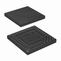
AT91SAM9G20B-CFU Atmel, AT91SAM9G20B-CFU Datasheet - Page 13

AT91SAM9G20B-CFU
Manufacturer Part Number
AT91SAM9G20B-CFU
Description
IC MCU ARM9 247-LFBGA
Manufacturer
Atmel
Series
AT91SAMr
Datasheet
1.AT91SAM9G20B-CU.pdf
(42 pages)
Specifications of AT91SAM9G20B-CFU
Core Processor
ARM9
Core Size
16/32-Bit
Speed
400MHz
Connectivity
EBI/EMI, Ethernet, I²C, IrDA, ISI, MMC, SPI, SSC, UART/USART, USB
Peripherals
DMA, POR, PWM, WDT
Number Of I /o
96
Program Memory Size
64KB (64K x 8)
Program Memory Type
ROM
Ram Size
96K x 8
Voltage - Supply (vcc/vdd)
0.9 V ~ 1.1 V
Data Converters
A/D 4x10b
Oscillator Type
Internal
Operating Temperature
-40°C ~ 85°C
Package / Case
247-TFBGA
Processor Series
AT91SAMx
Core
ARM926EJ-S
Data Bus Width
32 bit
Data Ram Size
16 KB
Interface Type
SPI, TWI, UART
Maximum Clock Frequency
400 MHz
Number Of Programmable I/os
96
Operating Supply Voltage
3.3 V
Maximum Operating Temperature
+ 85 C
Mounting Style
SMD/SMT
3rd Party Development Tools
JTRACE-ARM-2M, MDK-ARM, RL-ARM, ULINK2
Development Tools By Supplier
AT91SAM-ICE, AT91-ISP, AT91SAM9G20-EK
Minimum Operating Temperature
- 40 C
Lead Free Status / RoHS Status
Lead free / RoHS Compliant
Eeprom Size
-
Lead Free Status / Rohs Status
Details
Available stocks
Company
Part Number
Manufacturer
Quantity
Price
5. Power Considerations
5.1
5.2
6384DS–ATARM–13-Jan-10
Power Supplies
Programmable I/O Lines
The AT91SAM9G20 has several types of power supply pins:
Ground pins GND are common to VDDCORE, VDDIOM, VDDOSC and VDDIOP pins power
supplies. Separated ground pins are provided for VDDBU, VDDPLL, VDDUSB and VDDANA.
These ground pins are respectively GNDBU, GNDPLL, GNDUSB and GNDANA.
The power supplies pins VDDIOM accept two voltage ranges. This allows the device to reach its
maximum speed either out of 1.8V or 3.3V external memories.
The maximum speed is 133 MHz on the pin SDCK (SDRAM Clock) loaded with 10 pF. The other
signals (control, address and data signals) do not go over 66 MHz, loaded with 30 pF for power
supply at 1.8V and 50 pF for power supply at 3.3V.
The EBI I/Os accept two slew rate modes, Fast and Slow. This allows to adapt the rising and fall-
ing time on SDRAM clock, control and data to the bus load.
The voltage ranges and the slew rates are determined by programming VDDIOMSEL and IOSR
bits in the Chip Configuration registers located in the Matrix User Interface.
At reset, the selected voltage defaults to 3.3V nominal and power supply pins can accept either
1.8V or 3.3V. The user must make sure to program the EBI voltage range before getting the
device out of its Slow Clock Mode.
At reset, the selected slew rates defaults are Fast.
• VDDCORE pins: Power the core, including the processor, the embedded memories and the
• VDDIOM pins: Power the External Bus Interface I/O lines; voltage ranges between 1.65V and
• VDDIOP pins: Power the Peripherals I/O lines; voltage ranges from 1.65V to 3.6V.
• VDDBU pin: Powers the Slow Clock oscillator, the internal RC oscillator and a part of the
• VDDPLL pin: Powers the PLL cells; voltage ranges from 0.9V to 1.1V.
• VDDOSC pin: Powers the Main Oscillator cells; voltage ranges from 1.65V to 3.6V
• VDDANA pin: Powers the Analog to Digital Converter; voltage ranges from 3.0V to 3.6V, 3.3V
• VDDUSB pin: Powers USB transceiver; voltage ranges from 3.0V to 3.6V.
peripherals; voltage ranges from 0.9V to 1.1V, 1.0V nominal.
1.95V (1.8V typical) or between 3.0V and 3.6V (3.3V nominal). The voltage range is
selectable by software.
System Controller; voltage ranges from 0.9V to 1.1V, 1.0V nominal.
nominal.
AT91SAM9G20 Summary
13


