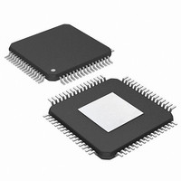
PIC24FJ256DA210-I/PT Microchip Technology, PIC24FJ256DA210-I/PT Datasheet - Page 354

PIC24FJ256DA210-I/PT
Manufacturer Part Number
PIC24FJ256DA210-I/PT
Description
MCU PIC 16BIT FLASH 256K 100TQFP
Manufacturer
Microchip Technology
Series
PIC® 24Fr
Specifications of PIC24FJ256DA210-I/PT
Core Size
16-Bit
Program Memory Size
256KB (85.5K x 24)
Core Processor
PIC
Speed
32MHz
Connectivity
I²C, IrDA, SPI, UART/USART, USB OTG
Peripherals
Brown-out Detect/Reset, GFX, LVD, POR, PWM, WDT
Number Of I /o
84
Program Memory Type
FLASH
Ram Size
96K x 8
Voltage - Supply (vcc/vdd)
2.2 V ~ 3.6 V
Data Converters
A/D 24x10b
Oscillator Type
Internal
Operating Temperature
-40°C ~ 85°C
Package / Case
100-TFQFP
Controller Family/series
PIC24
No. Of I/o's
84
Ram Memory Size
96KB
Cpu Speed
32MHz
No. Of Timers
5
Interface
I2C, SPI, UART, USB
Embedded Interface Type
I2C, SPI, UART, USB
Rohs Compliant
Yes
Processor Series
PIC24FJ
Core
PIC
Data Bus Width
16 bit
Data Ram Size
96 KB
Interface Type
UART, SPI, USB, I2C, RS-485, RS-232
Maximum Clock Frequency
32 MHz
Number Of Programmable I/os
23
Number Of Timers
5
Operating Supply Voltage
3.6 V
Maximum Operating Temperature
+ 85 C
Mounting Style
SMD/SMT
3rd Party Development Tools
52713-733, 52714-737, 53276-922, EWDSPIC
Development Tools By Supplier
PG164130, DV164035, DV244005, DV164005, AC164127-4, AC164127-6, AC164139, DM240001, DM240312, DV164039
Minimum Operating Temperature
- 40 C
Lead Free Status / RoHS Status
Lead free / RoHS Compliant
Eeprom Size
-
Lead Free Status / Rohs Status
Details
Available stocks
Company
Part Number
Manufacturer
Quantity
Price
Company:
Part Number:
PIC24FJ256DA210-I/PT
Manufacturer:
Microchip Technology
Quantity:
10 000
Part Number:
PIC24FJ256DA210-I/PT
Manufacturer:
MICROCHIP/微芯
Quantity:
20 000
- Current page: 354 of 408
- Download datasheet (4Mb)
PIC24FJ256DA210 FAMILY
REGISTER 27-6:
27.2
All PIC24FJ256DA210 family devices power their core
digital logic at a nominal 1.8V. This may create an issue
for designs that are required to operate at a higher
typical voltage, such as 3.3V. To simplify system
design, all devices in the PIC24FJ256DA210 family
incorporate an on-chip regulator that allows the device
to run its core logic from V
The regulator is controlled by the ENVREG pin. Tying V
to the pin enables the regulator, which in turn, provides
power to the core from the other V
ulator is enabled, a low-ESR capacitor (such as ceramic)
must be connected to the V
helps to maintain the stability of the regulator. The recom-
mended value for the filter capacitor (C
Section 30.1 “DC Characteristics”.
27.2.1
When the on-chip regulator is enabled, it provides a
constant voltage of 1.8V nominal to the digital core
logic.
The regulator can provide this level from a V
2.1V, all the way up to the device’s V
have the capability to boost V
vent “brown-out” conditions when the voltage drops too
low for the regulator, the Brown-out Reset occurs. Then
the regulator output follows V
drop of 300 mV.
To provide information about when the regulator
voltage starts reducing, the on-chip regulator includes
a simple Low-Voltage Detect circuit, which sets the
DS39969B-page 354
bit 23
bit 15
bit 7
Legend: R = Readable bit
bit 23-4
bit 3-0
U-0
U-0
U-0
—
—
—
On-Chip Voltage Regulator
VOLTAGE REGULATOR
LOW-VOLTAGE DETECTION
Unimplemented: Read as ‘0’
REV<3:0>: Device revision identifier bits
U-0
U-0
U-0
—
—
—
DEVREV: DEVICE REVISION REGISTER
DD
CAP
.
DD
DD
DD
pin (Figure 27-1). This
levels. In order to pre-
with a typical voltage
pins. When the reg-
U-0
U-0
U-0
DDMAX
—
—
—
EFC
) is provided in
. It does not
DD
of about
U-0
U-0
U-0
—
—
—
DD
U = Unimplemented bit
REV3
Low-Voltage Detect Interrupt Flag, LVDIF (IFS4<8>).
This can be used to generate an interrupt to trigger an
orderly shutdown.
FIGURE 27-1:
27.2.2
When the voltage regulator is enabled, it takes approx-
imately 10 s for it to generate output. During this time,
designated as T
T
operation after any power-down, including Sleep mode.
T
(RCON<8>) and the WUTSEL Configuration bits
(CW3<11:10>). Refer to Section 30.0 “Electrical
Characteristics” for more information on T
U-0
U-0
—
—
VREG
VREG
R
Note 1:
Regulator Enabled (ENVREG tied to V
(10 F typ)
is determined by the status of the VREGS bit
is applied every time the device resumes
C
EFC
ON-CHIP REGULATOR AND POR
This is a typical operating voltage. Refer to
Section 30.1 “DC Characteristics” for
the full operating ranges of V
REV2
U-0
U-0
3.3V
—
—
R
VREG
(1)
CONNECTIONS FOR THE
ON-CHIP REGULATOR
, code execution is disabled.
2010 Microchip Technology Inc.
V
ENVREG
V
V
DD
CAP
SS
PIC24FJXXXDA1/DA2
REV1
U-0
U-0
—
—
R
DD
.
DD
VREG
REV0
):
U-0
U-0
—
—
R
bit 16
.
bit 8
bit 0
Related parts for PIC24FJ256DA210-I/PT
Image
Part Number
Description
Manufacturer
Datasheet
Request
R

Part Number:
Description:
Manufacturer:
Microchip Technology Inc.
Datasheet:

Part Number:
Description:
Manufacturer:
Microchip Technology Inc.
Datasheet:

Part Number:
Description:
Manufacturer:
Microchip Technology Inc.
Datasheet:

Part Number:
Description:
Manufacturer:
Microchip Technology Inc.
Datasheet:

Part Number:
Description:
Manufacturer:
Microchip Technology Inc.
Datasheet:

Part Number:
Description:
Manufacturer:
Microchip Technology Inc.
Datasheet:

Part Number:
Description:
Manufacturer:
Microchip Technology Inc.
Datasheet:

Part Number:
Description:
Manufacturer:
Microchip Technology Inc.
Datasheet:


