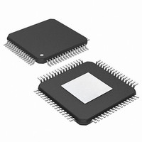
PIC24FJ256DA210-I/PT Microchip Technology, PIC24FJ256DA210-I/PT Datasheet - Page 309

PIC24FJ256DA210-I/PT
Manufacturer Part Number
PIC24FJ256DA210-I/PT
Description
MCU PIC 16BIT FLASH 256K 100TQFP
Manufacturer
Microchip Technology
Series
PIC® 24Fr
Specifications of PIC24FJ256DA210-I/PT
Core Size
16-Bit
Program Memory Size
256KB (85.5K x 24)
Core Processor
PIC
Speed
32MHz
Connectivity
I²C, IrDA, SPI, UART/USART, USB OTG
Peripherals
Brown-out Detect/Reset, GFX, LVD, POR, PWM, WDT
Number Of I /o
84
Program Memory Type
FLASH
Ram Size
96K x 8
Voltage - Supply (vcc/vdd)
2.2 V ~ 3.6 V
Data Converters
A/D 24x10b
Oscillator Type
Internal
Operating Temperature
-40°C ~ 85°C
Package / Case
100-TFQFP
Controller Family/series
PIC24
No. Of I/o's
84
Ram Memory Size
96KB
Cpu Speed
32MHz
No. Of Timers
5
Interface
I2C, SPI, UART, USB
Embedded Interface Type
I2C, SPI, UART, USB
Rohs Compliant
Yes
Processor Series
PIC24FJ
Core
PIC
Data Bus Width
16 bit
Data Ram Size
96 KB
Interface Type
UART, SPI, USB, I2C, RS-485, RS-232
Maximum Clock Frequency
32 MHz
Number Of Programmable I/os
23
Number Of Timers
5
Operating Supply Voltage
3.6 V
Maximum Operating Temperature
+ 85 C
Mounting Style
SMD/SMT
3rd Party Development Tools
52713-733, 52714-737, 53276-922, EWDSPIC
Development Tools By Supplier
PG164130, DV164035, DV244005, DV164005, AC164127-4, AC164127-6, AC164139, DM240001, DM240312, DV164039
Minimum Operating Temperature
- 40 C
Lead Free Status / RoHS Status
Lead free / RoHS Compliant
Eeprom Size
-
Lead Free Status / Rohs Status
Details
Available stocks
Company
Part Number
Manufacturer
Quantity
Price
Company:
Part Number:
PIC24FJ256DA210-I/PT
Manufacturer:
Microchip Technology
Quantity:
10 000
Part Number:
PIC24FJ256DA210-I/PT
Manufacturer:
MICROCHIP/微芯
Quantity:
20 000
- Current page: 309 of 408
- Download datasheet (4Mb)
REGISTER 22-5:
2010 Microchip Technology Inc.
bit 15
bit 7
Legend:
R = Readable bit
-n = Value at POR
bit 15-10
bit 9
bit 8
bit 7
bit 6
bit 5
bit 4
bit 3
bit 2
DPCLKPOL
R/W-0
U-0
—
Unimplemented: Read as ‘0’
DPPINOE: Display Pin Output Pad Enable bit
DPPINOE is the master output enable and must be set to allow GDBEN<15:0>, DPENOE,
DPPWROE, DPVSOE and DPHSOE to enable the associated pads
1 = Enable display output pads
0 = Disable display output signals as set by GDBEN<15:0>
Pins used by the signals are assigned to the next enabled module that uses the same pins.
For data signals, GDBEN<15:0> can be used to disable or enable specific data signals while
DPPINOE is set.
DPPOWER: Display Power-up Power-Down Sequencer Control bit
Refer to the “PIC24F Family Reference Manual”, Section 43. “Graphics Controller Module (GFX)”
for details.
1 = Set Display Power Sequencer Control port (GPWR) to ‘1’
0 = Set Power Control Sequencer signal (GPWR) ‘0’
DPCLKPOL: Display Glass Clock (GCLK) Polarity bit
1 = Display latches data on the positive edge of GCLK
0 = Display latches data on the negative edge of GCLK
DPENPOL: Display Enable Signal (GEN) Polarity bit
For TFT mode (DPMODE (G1CON2<2:0>) = 001):
1 = Active-high (GEN)
0 = Active-low (GEN)
For STN mode (DPMODE (G1CON2<2:0>) = 010 or 011):
1 = GEN connects to the shift clock input of the display (Shift Clock mode)
0 = GEN connects to the MOD input of the display (Line/Frame Toggle mode)
DPVSPOL: Display Vertical Synchronization (V
1 = Active-high (V
0 = Active-low (V
DPHSPOL: Display Horizontal Synchronization (HSYNC) Polarity bit
1 = Active-high (HSYNC)
0 = Active-low (HSYNC)
DPPWROE: Display Power-up/Power-Down Sequencer Control port (GPWR) enable bit
1 = GPWR port is enabled (pin controlled by the DPPOWER bit (G1CON3<8>))
0 = GPWR port is disabled (pin can be used as an ordinary I/O)
DPENOE: Display Enable Port Enable bit
1 = GEN port is enabled
0 = GEN port is disabled
DPENPOL
R/W-0
U-0
—
G1CON3: DISPLAY CONTROL REGISTER 3
W = Writable bit
‘1’ = Bit is set
SYNC
DPVSPOL
SYNC
R/W-0
U-0
—
)
)
PIC24FJ256DA210 FAMILY
DPHSPOL
R/W-0
U-0
—
SYNC
U = Unimplemented bit, read as ‘0’
DPPWROE
‘0’ = Bit is cleared
R/W-0
) Polarity bit
U-0
—
DPENOE
R/W-0
U-0
—
x = Bit is unknown
DPPINOE
DPVSOE
R/W-0
R/W-0
DS39969B-page 309
DPPOWER
DPHSOE
R/W-0
R/W-0
bit 8
bit 0
Related parts for PIC24FJ256DA210-I/PT
Image
Part Number
Description
Manufacturer
Datasheet
Request
R

Part Number:
Description:
Manufacturer:
Microchip Technology Inc.
Datasheet:

Part Number:
Description:
Manufacturer:
Microchip Technology Inc.
Datasheet:

Part Number:
Description:
Manufacturer:
Microchip Technology Inc.
Datasheet:

Part Number:
Description:
Manufacturer:
Microchip Technology Inc.
Datasheet:

Part Number:
Description:
Manufacturer:
Microchip Technology Inc.
Datasheet:

Part Number:
Description:
Manufacturer:
Microchip Technology Inc.
Datasheet:

Part Number:
Description:
Manufacturer:
Microchip Technology Inc.
Datasheet:

Part Number:
Description:
Manufacturer:
Microchip Technology Inc.
Datasheet:


