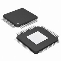
PIC24FJ256DA210-I/PT Microchip Technology, PIC24FJ256DA210-I/PT Datasheet - Page 150

PIC24FJ256DA210-I/PT
Manufacturer Part Number
PIC24FJ256DA210-I/PT
Description
MCU PIC 16BIT FLASH 256K 100TQFP
Manufacturer
Microchip Technology
Series
PIC® 24Fr
Specifications of PIC24FJ256DA210-I/PT
Core Size
16-Bit
Program Memory Size
256KB (85.5K x 24)
Core Processor
PIC
Speed
32MHz
Connectivity
I²C, IrDA, SPI, UART/USART, USB OTG
Peripherals
Brown-out Detect/Reset, GFX, LVD, POR, PWM, WDT
Number Of I /o
84
Program Memory Type
FLASH
Ram Size
96K x 8
Voltage - Supply (vcc/vdd)
2.2 V ~ 3.6 V
Data Converters
A/D 24x10b
Oscillator Type
Internal
Operating Temperature
-40°C ~ 85°C
Package / Case
100-TFQFP
Controller Family/series
PIC24
No. Of I/o's
84
Ram Memory Size
96KB
Cpu Speed
32MHz
No. Of Timers
5
Interface
I2C, SPI, UART, USB
Embedded Interface Type
I2C, SPI, UART, USB
Rohs Compliant
Yes
Processor Series
PIC24FJ
Core
PIC
Data Bus Width
16 bit
Data Ram Size
96 KB
Interface Type
UART, SPI, USB, I2C, RS-485, RS-232
Maximum Clock Frequency
32 MHz
Number Of Programmable I/os
23
Number Of Timers
5
Operating Supply Voltage
3.6 V
Maximum Operating Temperature
+ 85 C
Mounting Style
SMD/SMT
3rd Party Development Tools
52713-733, 52714-737, 53276-922, EWDSPIC
Development Tools By Supplier
PG164130, DV164035, DV244005, DV164005, AC164127-4, AC164127-6, AC164139, DM240001, DM240312, DV164039
Minimum Operating Temperature
- 40 C
Lead Free Status / RoHS Status
Lead free / RoHS Compliant
Eeprom Size
-
Lead Free Status / Rohs Status
Details
Available stocks
Company
Part Number
Manufacturer
Quantity
Price
Company:
Part Number:
PIC24FJ256DA210-I/PT
Manufacturer:
Microchip Technology
Quantity:
10 000
Part Number:
PIC24FJ256DA210-I/PT
Manufacturer:
MICROCHIP/微芯
Quantity:
20 000
- Current page: 150 of 408
- Download datasheet (4Mb)
PIC24FJ256DA210 FAMILY
FIGURE 8-2:
8.5.1
The system clock is generated from the 96 MHz branch
using a configurable postscaler/divider to generate a
range of frequencies for the system clock multiplexer.
The output of the multiplexer is further passed through
a fixed divide-by-3 divider and the final output is used
TABLE 8-2:
DS39969B-page 150
Note 1:
Input from
POSC
Input from
FRC
4 MHz or
8 MHz
These options are not compatible with USB operation. They may be used whenever the PLL branch is
selected and the USB module is disabled.
SYSTEM CLOCK GENERATION
FNOSC<2:0>
SYSTEM CLOCK OPTIONS FOR 96 MHz PLL BLOCK
MCU Clock Division
96 MHz PLL
(CPDIV<1:0>)
96 MHz PLL BLOCK
96 MHz
None (00)
PLL
2 (01)
4 (10)
8 (11)
4 MHz Branch
÷ 5
÷ 4
÷ 3
÷12
÷ 8
÷ 6
÷ 2
÷ 1
96 MHz Branch
PLLDIV<2:0>
111
110
101
100
011
010
001
000
Graphics Clock
Option 1
G1CLKSEL
as the system clock. Figure 8-2 shows this logic in the
system clock sub-block. Since the source is a 96 MHz
signal, the possible system clock frequencies are listed
in Table 8-2. The available system clock options are
always the same, regardless of the setting of the
PLLDIV Configuration bits.
48 MHz Branch
0
1
÷ 2
÷ 8
÷ 4
÷ 2
÷ 1
Graphics Clock
System Clock
USB Clock
CPDIV<1:0>
(Instruction Rate in MIPS)
System Clock Frequency
÷ 2
11
10
01
00
GCLKDIV<6:0>
32 MHz (16)
8 MHz (4)
4 MHz (2)
÷ 64
÷ 63
...
÷ 17.50
÷ 17.00
...
÷ 1.25
÷ 1
16 MHz (8)
Graphics Clock
Option 2
2010 Microchip Technology Inc.
127
126
...
65
64
...
1
0
÷ 3
.
.
.
(1)
(1)
48 MHz Clock
for USB Module
PLL Output for
System Clock
Clock Output for
Display Interface
(DISPCLK)
Clock Output
for Graphics
Controller
Module (G1CLK)
Related parts for PIC24FJ256DA210-I/PT
Image
Part Number
Description
Manufacturer
Datasheet
Request
R

Part Number:
Description:
Manufacturer:
Microchip Technology Inc.
Datasheet:

Part Number:
Description:
Manufacturer:
Microchip Technology Inc.
Datasheet:

Part Number:
Description:
Manufacturer:
Microchip Technology Inc.
Datasheet:

Part Number:
Description:
Manufacturer:
Microchip Technology Inc.
Datasheet:

Part Number:
Description:
Manufacturer:
Microchip Technology Inc.
Datasheet:

Part Number:
Description:
Manufacturer:
Microchip Technology Inc.
Datasheet:

Part Number:
Description:
Manufacturer:
Microchip Technology Inc.
Datasheet:

Part Number:
Description:
Manufacturer:
Microchip Technology Inc.
Datasheet:


