PIC24FJ256DA106-I/PT Microchip Technology, PIC24FJ256DA106-I/PT Datasheet - Page 83
PIC24FJ256DA106-I/PT
Manufacturer Part Number
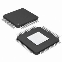
PIC24FJ256DA106-I/PT
Description
MCU PIC 16BIT FLASH 256K 64TQFP
Manufacturer
Microchip Technology
Series
PIC® 24Fr
Specifications of PIC24FJ256DA106-I/PT
Core Size
16-Bit
Program Memory Size
256KB (85.5K x 24)
Core Processor
PIC
Speed
32MHz
Connectivity
I²C, IrDA, SPI, UART/USART, USB OTG
Peripherals
Brown-out Detect/Reset, GFX, LVD, POR, PWM, WDT
Number Of I /o
52
Program Memory Type
FLASH
Ram Size
24K x 8
Voltage - Supply (vcc/vdd)
2.2 V ~ 3.6 V
Data Converters
A/D 16x10b
Oscillator Type
Internal
Operating Temperature
-40°C ~ 85°C
Package / Case
64-TFQFP
Controller Family/series
PIC24
No. Of I/o's
52
Ram Memory Size
24KB
Cpu Speed
32MHz
No. Of Timers
5
Interface
I2C, SPI, UART, USB
Embedded Interface Type
I2C, SPI, UART, USB
Rohs Compliant
Yes
Processor Series
PIC24FJ
Core
PIC
Data Bus Width
16 bit
Data Ram Size
24 KB
Interface Type
I2C, SPI, UART
Maximum Clock Frequency
32 MHz
Number Of Programmable I/os
29
Number Of Timers
5
Operating Supply Voltage
2.2 V to 3.6 V
Maximum Operating Temperature
+ 85 C
Mounting Style
SMD/SMT
3rd Party Development Tools
52713-733, 52714-737, 53276-922, EWDSPIC
Development Tools By Supplier
PG164130, DV164035, DV244005, DV164005, AC164127-4, AC164127-6, AC164139, DM240001, DM240312, DV164039
Minimum Operating Temperature
- 40 C
On-chip Adc
10 bit, 16 Channel
Lead Free Status / RoHS Status
Lead free / RoHS Compliant
Eeprom Size
-
Lead Free Status / Rohs Status
Details
Available stocks
Company
Part Number
Manufacturer
Quantity
Price
Company:

Part Number:
PIC24FJ256DA106-I/PT
Manufacturer:
Microchip Technology
Quantity:
10 000


REGISTER 5-1:
2010 Microchip Technology Inc.
bit 15
bit 7
Legend:
R = Readable bit
-n = Value at POR
HC = Hardware Clearable bit
bit 15
bit 14
bit 13
bit 12-7
bit 6
bit 5-4
bit 3-0
Note 1:
R/S-0, HC
WR
U-0
—
2:
3:
(1)
These bits can only be reset on POR.
All other combinations of NVMOP<3:0> are unimplemented.
Available in ICSP™ mode only; refer to the device programming specification.
WR: Write Control bit
1 = Initiates a Flash memory program or erase operation; the operation is self-timed and the bit is
0 = Program or erase operation is complete and inactive
WREN: Write Enable bit
1 = Enable Flash program/erase operations
0 = Inhibit Flash program/erase operations
WRERR: Write Sequence Error Flag bit
1 = An improper program or erase sequence attempt or termination has occurred (bit is set
0 = The program or erase operation completed normally
Unimplemented: Read as ‘0’
ERASE: Erase/Program Enable bit
1 = Perform the erase operation specified by NVMOP<3:0> on the next WR command
0 = Perform the program operation specified by NVMOP<3:0> on the next WR command
Unimplemented: Read as ‘0’
NVMOP<3:0>: NVM Operation Select bits
1111 = Memory bulk erase operation (ERASE = 1) or no operation (ERASE = 0)
0011 = Memory word program operation (ERASE = 0) or no operation (ERASE = 1)
0010 = Memory page erase operation (ERASE = 1) or no operation (ERASE = 0)
0001 = Memory row program operation (ERASE = 0) or no operation (ERASE = 1)
R/W-0
R/W-0
ERASE
WREN
cleared by hardware once the operation is complete
automatically on any set attempt of the WR bit)
NVMCON: FLASH MEMORY CONTROL REGISTER
(1)
(1)
S = Settable bit
W = Writable bit
‘1’ = Bit is set
R-0, HSC
WRERR
U-0
—
(1)
(1)
(1)
PIC24FJ256DA210 FAMILY
U-0
U-0
—
—
(1)
(1)
(1,2)
HSC = Hardware Settable/Clearable bit
U = Unimplemented bit, read as ‘0’
‘0’ = Bit is cleared
NVMOP3
R/W-0
U-0
—
(1)
(2)
NVMOP2
R/W-0
U-0
—
(1)
(2)
x = Bit is unknown
NVMOP1
R/W-0
U-0
—
(3)
(1)
(2)
DS39969B-page 83
NVMOP0
R/W-0
U-0
—
(1)
bit 8
bit 0
(2)
Related parts for PIC24FJ256DA106-I/PT
Image
Part Number
Description
Manufacturer
Datasheet
Request
R

Part Number:
Description:
Manufacturer:
Microchip Technology Inc.
Datasheet:
Part Number:
Description:
Manufacturer:
Microchip Technology Inc.
Datasheet:
Part Number:
Description:
Manufacturer:
Microchip Technology Inc.
Datasheet:
Part Number:
Description:
Manufacturer:
Microchip Technology Inc.
Datasheet:
Part Number:
Description:
Manufacturer:
Microchip Technology Inc.
Datasheet:
Part Number:
Description:
Manufacturer:
Microchip Technology Inc.
Datasheet:
Part Number:
Description:
Manufacturer:
Microchip Technology Inc.
Datasheet:
Part Number:
Description:
Manufacturer:
Microchip Technology Inc.
Datasheet: