PIC24FJ256DA106-I/PT Microchip Technology, PIC24FJ256DA106-I/PT Datasheet - Page 275
PIC24FJ256DA106-I/PT
Manufacturer Part Number
PIC24FJ256DA106-I/PT
Description
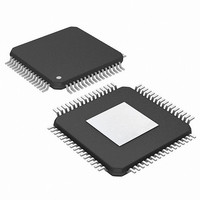
MCU PIC 16BIT FLASH 256K 64TQFP
Manufacturer
Microchip Technology
Series
PIC® 24Fr
Specifications of PIC24FJ256DA106-I/PT
Core Size
16-Bit
Program Memory Size
256KB (85.5K x 24)
Core Processor
PIC
Speed
32MHz
Connectivity
I²C, IrDA, SPI, UART/USART, USB OTG
Peripherals
Brown-out Detect/Reset, GFX, LVD, POR, PWM, WDT
Number Of I /o
52
Program Memory Type
FLASH
Ram Size
24K x 8
Voltage - Supply (vcc/vdd)
2.2 V ~ 3.6 V
Data Converters
A/D 16x10b
Oscillator Type
Internal
Operating Temperature
-40°C ~ 85°C
Package / Case
64-TFQFP
Controller Family/series
PIC24
No. Of I/o's
52
Ram Memory Size
24KB
Cpu Speed
32MHz
No. Of Timers
5
Interface
I2C, SPI, UART, USB
Embedded Interface Type
I2C, SPI, UART, USB
Rohs Compliant
Yes
Processor Series
PIC24FJ
Core
PIC
Data Bus Width
16 bit
Data Ram Size
24 KB
Interface Type
I2C, SPI, UART
Maximum Clock Frequency
32 MHz
Number Of Programmable I/os
29
Number Of Timers
5
Operating Supply Voltage
2.2 V to 3.6 V
Maximum Operating Temperature
+ 85 C
Mounting Style
SMD/SMT
3rd Party Development Tools
52713-733, 52714-737, 53276-922, EWDSPIC
Development Tools By Supplier
PG164130, DV164035, DV244005, DV164005, AC164127-4, AC164127-6, AC164139, DM240001, DM240312, DV164039
Minimum Operating Temperature
- 40 C
On-chip Adc
10 bit, 16 Channel
Lead Free Status / RoHS Status
Lead free / RoHS Compliant
Eeprom Size
-
Lead Free Status / Rohs Status
Details
Available stocks
Company
Part Number
Manufacturer
Quantity
Price
Company:

Part Number:
PIC24FJ256DA106-I/PT
Manufacturer:
Microchip Technology
Quantity:
10 000


REGISTER 19-1:
2010 Microchip Technology Inc.
bit 15
bit 7
Legend:
R = Readable bit
-n = Value at POR
bit 15
bit 14
bit 13
bit 12-11
bit 10
bit 9-8
bit 7-6
bit 5
bit 4
bit 3
bit 2
bit 1-0
PMPEN
R/W-0
R/W-0
CSF1
PMPEN: Parallel Master Port Enable bit
1 = EPMP is enabled
0 = EPMP is disabled
Unimplemented: Read as ‘0’
PSIDL: Stop in Idle Mode bit
1 = Discontinue module operation when device enters Idle mode
0 = Continue module operation in Idle mode
ADRMUX<1:0>: Address/Data Multiplexing Selection bits
11 = Lower address bits are multiplexed with data bits using 3 address phases
10 = Lower address bits are multiplexed with data bits using 2 address phases
01 = Lower address bits are multiplexed with data bits using 1 address phase
00 = Address and data appear on separate pins
Unimplemented: Read as ‘0’
MODE<1:0>: Parallel Port Mode Select bits
11 = Master mode
10 = Enhanced PSP; pins used are PMRD, PMWR, PMCS, PMD<7:0> and PMA<1:0>
01 = Buffered PSP; pins used are PMRD, PMWR, PMCS and PMD<7:0>
00 = Legacy Parallel Slave Port; PMRD, PMWR, PMCS and PMD<7:0> pins are used
CSF<1:0>: Chip Select Function bits
11 = Reserved
10 = PMA<15> used for Chip Select 2, PMA<14> used for Chip Select 1
01 = PMA<15> used for Chip Select 2, PMCS1 used for Chip Select 1
00 = PMCS2 used for Chip Select 2, PMCS1 used for Chip Select 1
ALP: Address Latch Polarity bit
1 = Active-high (PMALL, PMALH and PMALU)
0 = Active-low (PMALL, PMALH and PMALU)
ALMODE: Address Latch Strobe Mode bit
1 = Enable “smart” address strobes (each address phase is only present if the current access would
0 = Disable “smart” address strobes
Unimplemented: Read as ‘0’
BUSKEEP: Bus Keeper bit
1 = Data bus keeps its last value when not actively being driven
0 = Data bus is in high-impedance state when not actively being driven
IRQM<1:0>: Interrupt Request Mode bits
11 = Interrupt generated when Read Buffer 3 is read or Write Buffer 3 is written (Buffered PSP mode),
10 = Reserved
01 = Interrupt generated at the end of a read/write cycle
00 = No interrupt is generated
R/W-0
CSF0
U-0
cause a different address in the latch than the previous address)
—
or on a read or write operation when PMA<1:0> = 11 (Addressable PSP mode only)
PMCON1: EPMP CONTROL REGISTER 1
W = Writable bit
‘1’ = Bit is set
R/W-0
PSIDL
R/W-0
ALP
ADRMUX1
ALMODE
PIC24FJ256DA210 FAMILY
R/W-0
R/W-0
U = Unimplemented bit, read as ‘0’
‘0’ = Bit is cleared
ADRMUX0
R/W-0
U-0
—
BUSKEEP
R/W-0
U-0
—
x = Bit is unknown
MODE1
IRQM1
R/W-0
R/W-0
DS39969B-page 275
MODE0
IRQM0
R/W-0
R/W-0
bit 8
bit 0
Related parts for PIC24FJ256DA106-I/PT
Image
Part Number
Description
Manufacturer
Datasheet
Request
R

Part Number:
Description:
Manufacturer:
Microchip Technology Inc.
Datasheet:
Part Number:
Description:
Manufacturer:
Microchip Technology Inc.
Datasheet:
Part Number:
Description:
Manufacturer:
Microchip Technology Inc.
Datasheet:
Part Number:
Description:
Manufacturer:
Microchip Technology Inc.
Datasheet:
Part Number:
Description:
Manufacturer:
Microchip Technology Inc.
Datasheet:
Part Number:
Description:
Manufacturer:
Microchip Technology Inc.
Datasheet:
Part Number:
Description:
Manufacturer:
Microchip Technology Inc.
Datasheet:
Part Number:
Description:
Manufacturer:
Microchip Technology Inc.
Datasheet: