PIC24FJ256DA106-I/PT Microchip Technology, PIC24FJ256DA106-I/PT Datasheet - Page 351
PIC24FJ256DA106-I/PT
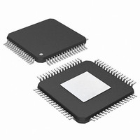
Manufacturer Part Number
PIC24FJ256DA106-I/PT
Description
MCU PIC 16BIT FLASH 256K 64TQFP
Manufacturer
Microchip Technology
Series
PIC® 24Fr
Specifications of PIC24FJ256DA106-I/PT
Core Size
16-Bit
Program Memory Size
256KB (85.5K x 24)
Core Processor
PIC
Speed
32MHz
Connectivity
I²C, IrDA, SPI, UART/USART, USB OTG
Peripherals
Brown-out Detect/Reset, GFX, LVD, POR, PWM, WDT
Number Of I /o
52
Program Memory Type
FLASH
Ram Size
24K x 8
Voltage - Supply (vcc/vdd)
2.2 V ~ 3.6 V
Data Converters
A/D 16x10b
Oscillator Type
Internal
Operating Temperature
-40°C ~ 85°C
Package / Case
64-TFQFP
Controller Family/series
PIC24
No. Of I/o's
52
Ram Memory Size
24KB
Cpu Speed
32MHz
No. Of Timers
5
Interface
I2C, SPI, UART, USB
Embedded Interface Type
I2C, SPI, UART, USB
Rohs Compliant
Yes
Processor Series
PIC24FJ
Core
PIC
Data Bus Width
16 bit
Data Ram Size
24 KB
Interface Type
I2C, SPI, UART
Maximum Clock Frequency
32 MHz
Number Of Programmable I/os
29
Number Of Timers
5
Operating Supply Voltage
2.2 V to 3.6 V
Maximum Operating Temperature
+ 85 C
Mounting Style
SMD/SMT
3rd Party Development Tools
52713-733, 52714-737, 53276-922, EWDSPIC
Development Tools By Supplier
PG164130, DV164035, DV244005, DV164005, AC164127-4, AC164127-6, AC164139, DM240001, DM240312, DV164039
Minimum Operating Temperature
- 40 C
On-chip Adc
10 bit, 16 Channel
Lead Free Status / RoHS Status
Lead free / RoHS Compliant
Eeprom Size
-
Lead Free Status / Rohs Status
Details
Available stocks
Company
Part Number
Manufacturer
Quantity
Price
Company:

Part Number:
PIC24FJ256DA106-I/PT
Manufacturer:
Microchip Technology
Quantity:
10 000


REGISTER 27-2:
REGISTER 27-3:
2010 Microchip Technology Inc.
bit 4
bit 3-2
bit 1-0
bit 23
bit 15
bit 7
Legend:
R = Readable bit
-n = Value at POR
bit 23-16
bit 15
bit 14
bit 13
bit 12
Note 1:
WPEND
WPFP7
R/PO-1
R/PO-1
U-0
—
2:
3:
Unimplemented in 64-pin devices, maintain at ‘1’.
Ensure that the SCLKI pin is made a digital input while using this configuration, see Table 10-1.
Regardless of WPCFG status, if WPEND = 1 or if WPFP corresponds to the Configuration Word’s page,
the Configuration Word’s page is protected.
IOL1WAY: IOLOCK One-Way Set Enable bit
1 = The IOLOCK bit (OSCCON<6>) can be set once, provided the unlock sequence has been
0 = The IOLOCK bit can be set and cleared as needed, provided the unlock sequence has been
Reserved: Always maintain as ‘1’
POSCMD<1:0>: Primary Oscillator Configuration bits
11 = Primary oscillator is disabled
10 = HS Oscillator mode is selected
01 = XT Oscillator mode is selected
00 = EC Oscillator mode is selected
Unimplemented: Read as ‘1’
WPEND: Segment Write Protection End Page Select bit
1 = Protected code segment upper boundary is at the last page of program memory; the lower
0 = Protected code segment lower boundary is at the bottom of the program memory (000000h); upper
WPCFG: Configuration Word Code Page Write Protection Select bit
1 = Last page (at the top of program memory) and Flash Configuration Words are not write-protected
0 = Last page and Flash Configuration Words are write-protected, provided WPDIS = ‘0’
WPDIS: Segment Write Protection Disable bit
1 = Segmented code protection is disabled
0 = Segmented code protection is enabled; protected segment is defined by the WPEND, WPCFG and
ALTPMP: Alternate EPMP Pin Mapping bit
1 = EPMP pins are in default location mode
0 = EPMP pins are in alternate location mode
WPCFG
WPFP6
R/PO-1
R/PO-1
completed. Once set, the Peripheral Pin Select registers cannot be written to a second time.
completed
boundary is the code page specified by WPFP<7:0>
boundary is the code page specified by WPFP<7:0>
WPFPx Configuration bits
U-0
—
CW2: FLASH CONFIGURATION WORD 2 (CONTINUED)
CW3: FLASH CONFIGURATION WORD 3
PO = Program-Once bit
W = Writable bit
‘1’ = Bit is set
WPFP5
R/PO-1
R/PO-1
WPDIS
U-0
—
ALTPMP
PIC24FJ256DA210 FAMILY
WPFP4
R/PO-1
R/PO-1
U-0
—
(1)
(1)
U = Unimplemented bit, read as ‘0’
‘0’ = Bit is cleared
WUTSEL1
R/PO-1
R/PO-1
WPFP3
U-0
—
WUTSEL0
WPFP2
R/PO-1
R/PO-1
U-0
—
x = Bit is unknown
SOSCSEL1
WPFP1
R/PO-1
R/PO-1
U-0
—
DS39969B-page 351
SOSCSEL0
WPFP0
R/PO-1
R/PO-1
U-0
—
bit 16
bit 8
bit 0
(3)
Related parts for PIC24FJ256DA106-I/PT
Image
Part Number
Description
Manufacturer
Datasheet
Request
R

Part Number:
Description:
Manufacturer:
Microchip Technology Inc.
Datasheet:
Part Number:
Description:
Manufacturer:
Microchip Technology Inc.
Datasheet:
Part Number:
Description:
Manufacturer:
Microchip Technology Inc.
Datasheet:
Part Number:
Description:
Manufacturer:
Microchip Technology Inc.
Datasheet:
Part Number:
Description:
Manufacturer:
Microchip Technology Inc.
Datasheet:
Part Number:
Description:
Manufacturer:
Microchip Technology Inc.
Datasheet:
Part Number:
Description:
Manufacturer:
Microchip Technology Inc.
Datasheet:
Part Number:
Description:
Manufacturer:
Microchip Technology Inc.
Datasheet: