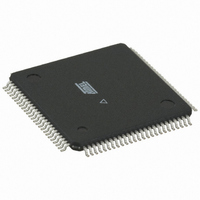
ATMEGA3250V-8AU Atmel, ATMEGA3250V-8AU Datasheet - Page 185

ATMEGA3250V-8AU
Manufacturer Part Number
ATMEGA3250V-8AU
Description
IC AVR MCU 32K 8MHZ 100TQFP
Manufacturer
Atmel
Series
AVR® ATmegar
Specifications of ATMEGA3250V-8AU
Core Processor
AVR
Core Size
8-Bit
Speed
8MHz
Connectivity
SPI, UART/USART, USI
Peripherals
Brown-out Detect/Reset, POR, PWM, WDT
Number Of I /o
69
Program Memory Size
32KB (16K x 16)
Program Memory Type
FLASH
Eeprom Size
1K x 8
Ram Size
2K x 8
Voltage - Supply (vcc/vdd)
1.8 V ~ 5.5 V
Data Converters
A/D 8x10b
Oscillator Type
Internal
Operating Temperature
-40°C ~ 85°C
Package / Case
100-TQFP, 100-VQFP
Processor Series
ATMEGA32x
Core
AVR8
Data Bus Width
8 bit
Data Ram Size
2 KB
Interface Type
SPI, UART, USI
Maximum Clock Frequency
8 MHz
Number Of Programmable I/os
69
Number Of Timers
3
Operating Supply Voltage
1.8 V to 5.5 V
Maximum Operating Temperature
+ 85 C
Mounting Style
SMD/SMT
Minimum Operating Temperature
- 40 C
On-chip Adc
10 bit, 8 Channel
Package
100TQFP
Device Core
AVR
Family Name
ATmega
Maximum Speed
8 MHz
For Use With
ATSTK600-TQFP100 - STK600 SOCKET/ADAPTER 100-TQFP770-1007 - ISP 4PORT ATMEL AVR MCU SPI/JTAG770-1005 - ISP 4PORT FOR ATMEL AVR MCU JTAG770-1004 - ISP 4PORT FOR ATMEL AVR MCU SPIATAVRISP2 - PROGRAMMER AVR IN SYSTEMATSTK504 - STARTER KIT AVR EXP MOD 100P LCD
Lead Free Status / RoHS Status
Lead free / RoHS Compliant
Available stocks
Company
Part Number
Manufacturer
Quantity
Price
Part Number:
ATMEGA3250V-8AU
Manufacturer:
ATMEL/爱特梅尔
Quantity:
20 000
- Current page: 185 of 362
- Download datasheet (7Mb)
20. USI – Universal Serial Interface
20.1
2570M–AVR–04/11
Overview
The Universal Serial Interface, or USI, provides the basic hardware resources needed for serial
communication. Combined with a minimum of control software, the USI allows significantly
higher transfer rates and uses less code space than solutions based on software only. Interrupts
are included to minimize the processor load. The main features of the USI are:
•
•
•
•
•
•
A simplified block diagram of the USI is shown on Figure 20-1. For the actual placement of I/O
pins, refer to
CPU accessible I/O Registers, including I/O bits and I/O pins, are shown in bold. The device-
specific I/O Register and bit locations are listed in the
Figure 20-1. Universal Serial Interface, Block Diagram
The 8-bit Shift Register is directly accessible via the data bus and contains the incoming and
outgoing data. The register has no buffering so the data must be read as quickly as possible to
ensure that no data is lost. The most significant bit is connected to one of two output pins
depending of the wire mode configuration. A transparent latch is inserted between the Serial
Register Output and output pin, which delays the change of data output to the opposite clock
edge of the data input sampling. The serial input is always sampled from the Data Input (DI) pin
independent of the configuration.
The 4-bit counter can be both read and written via the data bus, and can generate an overflow
interrupt. Both the Serial Register and the counter are clocked simultaneously by the same clock
source. This allows the counter to count the number of bits received or transmitted and generate
Two-wire Synchronous Data Transfer (Master or Slave)
Three-wire Synchronous Data Transfer (Master or Slave)
Data Received Interrupt
Wake up from Idle Mode
In Two-wire Mode: Wake-up from All Sleep Modes, Including Power-down Mode
Two-wire Start Condition Detector with Interrupt Capability
“Pinout ATmega3250/6450” on page 2
USIDR
USICR
USISR
2
4-bit Counter
3
2
1
0
3
2
1
0
D Q
LE
ATmega325/3250/645/6450
[1]
TIM0 COMP
0
1
and
“Register Descriptions” on page
“Pinout ATmega325/645” on page
Two-wire Clock
Control Unit
CLOCK
HOLD
DO
DI/SDA
USCK/SCL
(Output only)
(Input/Open Drain)
(Input/Open Drain)
192.
185
3.
Related parts for ATMEGA3250V-8AU
Image
Part Number
Description
Manufacturer
Datasheet
Request
R

Part Number:
Description:
Manufacturer:
Atmel Corporation
Datasheet:

Part Number:
Description:
IC AVR MCU 32K 16MHZ 64-QFN
Manufacturer:
Atmel
Datasheet:

Part Number:
Description:
IC AVR MCU 32K 16MHZ 64TQFP
Manufacturer:
Atmel
Datasheet:

Part Number:
Description:
IC AVR MCU 32K 16MHZ 64TQFP
Manufacturer:
Atmel
Datasheet:

Part Number:
Description:
IC AVR MCU 32K 16MHZ 64-QFN
Manufacturer:
Atmel
Datasheet:

Part Number:
Description:
8-bit Microcontroller with In-System Programmable Flash
Manufacturer:
ATMEL [ATMEL Corporation]
Datasheet:

Part Number:
Description:
MCU AVR 32K FLASH 16MHZ 64TQFP
Manufacturer:
Atmel
Datasheet:

Part Number:
Description:
MCU AVR 32K FLASH 16MHZ 64QFN
Manufacturer:
Atmel
Datasheet:

Part Number:
Description:
Manufacturer:
Atmel Corporation
Datasheet:

Part Number:
Description:
Manufacturer:
ATMEL Corporation
Datasheet:

Part Number:
Description:
IC AVR MCU 32K 16MHZ 5V 44-QFN
Manufacturer:
Atmel
Datasheet:

Part Number:
Description:
IC AVR MCU 32K 16MHZ 5V 40DIP
Manufacturer:
Atmel
Datasheet:

Part Number:
Description:
IC AVR MCU 32K 16MHZ 5V 44TQFP
Manufacturer:
Atmel
Datasheet:


