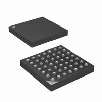
ATXMEGA32A4-CU Atmel, ATXMEGA32A4-CU Datasheet - Page 227

ATXMEGA32A4-CU
Manufacturer Part Number
ATXMEGA32A4-CU
Description
MCU AVR 32+4 FLASH 49VFBGA
Manufacturer
Atmel
Series
AVR® XMEGAr
Specifications of ATXMEGA32A4-CU
Core Processor
AVR
Core Size
8/16-Bit
Speed
32MHz
Connectivity
I²C, IrDA, SPI, UART/USART
Peripherals
Brown-out Detect/Reset, DMA, POR, PWM, WDT
Number Of I /o
34
Program Memory Size
32KB (16K x 16)
Program Memory Type
FLASH
Eeprom Size
2K x 8
Ram Size
4K x 8
Voltage - Supply (vcc/vdd)
1.6 V ~ 3.6 V
Data Converters
A/D 12x12b, D/A 2x12b
Oscillator Type
Internal
Operating Temperature
-40°C ~ 85°C
Package / Case
49-VFBGA
Processor Series
ATXMEGA32x
Core
AVR8
Data Bus Width
8 bit, 16 bit
Data Ram Size
4 KB
Interface Type
I2C, SPI, USART
Maximum Clock Frequency
32 MHz
Number Of Programmable I/os
36
Number Of Timers
5
Operating Supply Voltage
1.6 V to 3.6 V
Maximum Operating Temperature
+ 85 C
Mounting Style
SMD/SMT
3rd Party Development Tools
EWAVR, EWAVR-BL
Development Tools By Supplier
ATAVRDRAGON, ATAVRISP2, ATAVRONEKIT
Minimum Operating Temperature
- 40 C
On-chip Adc
12 bit, 1 Channel
On-chip Dac
2 bit, 1 Channel
For Use With
ATAVRONEKIT - KIT AVR/AVR32 DEBUGGER/PROGRMMRATSTK600 - DEV KIT FOR AVR/AVR32770-1007 - ISP 4PORT ATMEL AVR MCU SPI/JTAG770-1004 - ISP 4PORT FOR ATMEL AVR MCU SPI
Lead Free Status / RoHS Status
Lead free / RoHS Compliant
Available stocks
Company
Part Number
Manufacturer
Quantity
Price
- Current page: 227 of 445
- Download datasheet (6Mb)
19.10.6
8077H–AVR–12/09
ADDRMASK - TWI Slave Address Mask Register
Accessing the DATA register will clear the slave interrupt flags and the CLKHOLD flag.
• Bit 7:1 - ADDRMASK[7:1]: Read/Write Direction
These bits in the ADDRMASK register can act as a second address match register, or an
address mask register depending on the ADDREN setting.
If ADDREN is set to zero, ADDRMASK can be loaded with a 7-bit Slave Address mask. Each bit
in ADDRMASK can mask (disable) the corresponding address bit in the ADDR register. If the
mask bit is one the address match between the incoming address bit and the corresponding bit
in ADDR is ignored, i.e. masked bits will always match.
If ADDREN is set to one, ADDRMASK can be loaded with a second slave address in addition to
the ADDR register. In this mode, the slave will match on 2 unique addresses, one in ADDR and
the other in ADDRMASK.
• Bit 0- ADDREN: Address Enable
By default this bit is zero and the ADDRMASK bits acts as an address mask to the ADDR regis-
ter. If this bit is set to one, the slave address match logic responds to the 2 unique addresses in
ADDR and ADDRMASK.
Bit
+0x05
Read/Write
Initial Value
R/W
7
0
R/W
6
0
R/W
5
0
ADDRMASK[7:1]
R/W
4
0
R/W
3
0
R/W
2
0
R/W
1
0
XMEGA A
ADDREN
R/W
0
0
ADDRMASK
227
Related parts for ATXMEGA32A4-CU
Image
Part Number
Description
Manufacturer
Datasheet
Request
R

Part Number:
Description:
DEV KIT FOR AVR/AVR32
Manufacturer:
Atmel
Datasheet:

Part Number:
Description:
INTERVAL AND WIPE/WASH WIPER CONTROL IC WITH DELAY
Manufacturer:
ATMEL Corporation
Datasheet:

Part Number:
Description:
Low-Voltage Voice-Switched IC for Hands-Free Operation
Manufacturer:
ATMEL Corporation
Datasheet:

Part Number:
Description:
MONOLITHIC INTEGRATED FEATUREPHONE CIRCUIT
Manufacturer:
ATMEL Corporation
Datasheet:

Part Number:
Description:
AM-FM Receiver IC U4255BM-M
Manufacturer:
ATMEL Corporation
Datasheet:

Part Number:
Description:
Monolithic Integrated Feature Phone Circuit
Manufacturer:
ATMEL Corporation
Datasheet:

Part Number:
Description:
Multistandard Video-IF and Quasi Parallel Sound Processing
Manufacturer:
ATMEL Corporation
Datasheet:

Part Number:
Description:
High-performance EE PLD
Manufacturer:
ATMEL Corporation
Datasheet:

Part Number:
Description:
8-bit Flash Microcontroller
Manufacturer:
ATMEL Corporation
Datasheet:

Part Number:
Description:
2-Wire Serial EEPROM
Manufacturer:
ATMEL Corporation
Datasheet:


