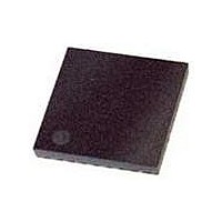
ATMEGA168-15MZ Atmel, ATMEGA168-15MZ Datasheet - Page 241

ATMEGA168-15MZ
Manufacturer Part Number
ATMEGA168-15MZ
Description
MCU AVR 16K FLASH 15MHZ 32-QFN
Manufacturer
Atmel
Series
AVR® ATmegar
Datasheet
1.ATMEGA168-15MZ.pdf
(340 pages)
Specifications of ATMEGA168-15MZ
Package / Case
32-VQFN Exposed Pad, 32-HVQFN, 32-SQFN, 32-DHVQFN
Voltage - Supply (vcc/vdd)
2.7 V ~ 5.5 V
Operating Temperature
-40°C ~ 125°C
Speed
16MHz
Number Of I /o
23
Eeprom Size
512 x 8
Core Processor
AVR
Program Memory Type
FLASH
Ram Size
1K x 8
Program Memory Size
16KB (16K x 8)
Data Converters
A/D 8x10b
Oscillator Type
Internal
Peripherals
Brown-out Detect/Reset, POR, PWM, WDT
Connectivity
I²C, SPI, UART/USART
Core Size
8-Bit
Processor Series
ATMEGA16x
Core
AVR8
Data Bus Width
8 bit
Data Ram Size
1 KB
Interface Type
2-Wire, SPI, USART, Serial
Maximum Clock Frequency
20 MHz
Number Of Programmable I/os
23
Number Of Timers
3
Maximum Operating Temperature
+ 85 C
Mounting Style
SMD/SMT
3rd Party Development Tools
EWAVR, EWAVR-BL
Development Tools By Supplier
ATAVRDRAGON, ATSTK500, ATSTK600, ATAVRISP2, ATAVRONEKIT
Minimum Operating Temperature
- 40 C
On-chip Adc
10 bit, 8 Channel
Package
32QFN EP
Device Core
AVR
Family Name
ATmega
Maximum Speed
16 MHz
Operating Supply Voltage
3.3|5 V
Lead Free Status / RoHS Status
Lead free / RoHS Compliant
Available stocks
Company
Part Number
Manufacturer
Quantity
Price
Company:
Part Number:
ATMEGA168-15MZ
Manufacturer:
ATMEL
Quantity:
1 300
Part Number:
ATMEGA168-15MZ
Manufacturer:
ATMEL/爱特梅尔
Quantity:
20 000
- Current page: 241 of 340
- Download datasheet (6Mb)
7530I–AVR–02/10
When Auto Triggering is used, the prescaler is reset when the trigger event occurs. This assures
a fixed delay from the trigger event to the start of conversion. In this mode, the sample-and-hold
takes place two ADC clock cycles after the rising edge on the trigger source signal. Three addi-
tional CPU clock cycles are used for synchronization logic.
In Free Running mode, a new conversion will be started immediately after the conversion com-
pletes, while ADSC remains high. For a summary of conversion times, see
Figure 21-4. ADC Timing Diagram, First Conversion (Single Conversion Mode)
Figure 21-5. ADC Timing Diagram, Single Conversion
Cycle Number
ADC Clock
ADSC
ADIF
ADCH
ADCL
Cycle Number
ADC Clock
ADEN
ADSC
ADIF
ADCH
ADCL
1
1
2
MUX and REFS
Update
2
MUX and REFS
Update
12
3
13
Sample & Hold
4
14
5
15
ATmega48/88/168 Automotive
6
Sample & Hold
16
First Conversion
17
7
One Conversion
18
8
19
9
20
10
Conversion
Complete
21
11
22
Conversion
Complete
23
12
24
13
25
Sign and MSB of Result
Sign and MSB of Result
Table
LSB of Result
Next Conversion
1
Next
Conversion
1
LSB of Result
2
2
21-1.
MUX and REFS
Update
MUX and REFS
Update
3
3
241
Related parts for ATMEGA168-15MZ
Image
Part Number
Description
Manufacturer
Datasheet
Request
R

Part Number:
Description:
Manufacturer:
Atmel Corporation
Datasheet:

Part Number:
Description:
Manufacturer:
Atmel Corporation
Datasheet:

Part Number:
Description:
Manufacturer:
ATMEL Corporation
Datasheet:

Part Number:
Description:
IC AVR MCU 16K 20MHZ 32TQFP
Manufacturer:
Atmel
Datasheet:

Part Number:
Description:
IC AVR MCU 16K 20MHZ 32-QFN
Manufacturer:
Atmel
Datasheet:

Part Number:
Description:
IC AVR MCU 16K 20MHZ 28DIP
Manufacturer:
Atmel
Datasheet:

Part Number:
Description:
MCU AVR 16K FLASH 15MHZ 32-TQFP
Manufacturer:
Atmel
Datasheet:

Part Number:
Description:
IC AVR MCU 16K 20MHZ 32TQFP
Manufacturer:
Atmel
Datasheet:

Part Number:
Description:
MCU AVR 16KB FLASH 20MHZ 32QFN
Manufacturer:
Atmel
Datasheet:

Part Number:
Description:
MCU AVR 16KB FLASH 20MHZ 32TQFP
Manufacturer:
Atmel
Datasheet:

Part Number:
Description:
IC MCU AVR 16K FLASH 32-QFN
Manufacturer:
Atmel
Datasheet:


