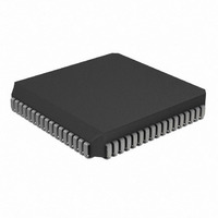
PIC16LC924-04I/L Microchip Technology, PIC16LC924-04I/L Datasheet - Page 15

PIC16LC924-04I/L
Manufacturer Part Number
PIC16LC924-04I/L
Description
IC MCU OTP 4KX14 LCD DVR 68PLCC
Manufacturer
Microchip Technology
Series
PIC® 16Cr
Specifications of PIC16LC924-04I/L
Core Processor
PIC
Core Size
8-Bit
Speed
4MHz
Connectivity
I²C, SPI
Peripherals
LCD, POR, PWM, WDT
Number Of I /o
25
Program Memory Size
7KB (4K x 14)
Program Memory Type
OTP
Ram Size
176 x 8
Voltage - Supply (vcc/vdd)
2.5 V ~ 6 V
Data Converters
A/D 5x8b
Oscillator Type
External
Operating Temperature
-40°C ~ 85°C
Package / Case
68-PLCC
Core
PIC
Processor Series
PIC16LC
Data Bus Width
8 bit
Maximum Clock Frequency
8 MHz
Data Ram Size
176 B
Data Rom Size
176 B
On-chip Adc
8 bit, 5 Channel
Number Of Programmable I/os
25
Number Of Timers
3
Operating Supply Voltage
2.5 V to 6 V
Mounting Style
SMD/SMT
Height
4.06 mm
Interface Type
I2C, SPI
Length
24.33 mm
Maximum Operating Temperature
+ 85 C
Minimum Operating Temperature
- 40 C
Supply Voltage (max)
6 V
Supply Voltage (min)
2.5 V
Width
24.33 mm
Lead Free Status / RoHS Status
Lead free / RoHS Compliant
Eeprom Size
-
Lead Free Status / Rohs Status
Details
Available stocks
Company
Part Number
Manufacturer
Quantity
Price
Company:
Part Number:
PIC16LC924-04I/L
Manufacturer:
Microchip Technology
Quantity:
10 000
3.1
The clock input (from OSC1) is internally divided by
four to generate four non-overlapping quadrature
clocks namely Q1, Q2, Q3 and Q4. Internally, the pro-
gram counter (PC) is incremented every Q1, the
instruction is fetched from the program memory and
latched into the instruction register in Q4. The instruc-
tion is decoded and executed during the following Q1
through Q4. The clocks and instruction execution flow
is shown in Figure 3-3.
FIGURE 3-3: CLOCK/INSTRUCTION CYCLE
EXAMPLE 3-1:
1. MOVLW 55h
2. MOVWF PORTB
3. CALL
4. BSF
5. Instruction @ address SUB_1
1997 Microchip Technology Inc.
All instructions are single cycle, except for any program branches. These take two cycles since the fetch
instruction is “flushed” from the pipeline while the new instruction is being fetched and then executed.
OSC2/CLKOUT
Clocking Scheme/Instruction Cycle
(RC mode)
SUB_1
PORTA, BIT3 (Forced NOP)
OSC1
Q4
PC
Q2
Q3
Q1
INSTRUCTION PIPELINE FLOW
Q1
Execute INST (PC-1)
Fetch INST (PC)
Q2
Fetch 1
Tcy0
PC
Q3
Q4
Execute 1
Fetch 2
Tcy1
Q1
Execute INST (PC)
Fetch INST (PC+1)
Q2
Execute 2
Fetch 3
PC+1
Tcy2
3.2
An “Instruction Cycle” consists of four Q cycles (Q1,
Q2, Q3 and Q4). The instruction fetch and execute are
pipelined such that fetch takes one instruction cycle
while decode and execute takes another instruction
cycle. However, due to the pipelining, each instruction
effectively executes in one cycle. If an instruction
causes the program counter to change (e.g. GOTO)
then two cycles are required to complete the instruction
(Example 3-1).
A fetch cycle begins with the program counter (PC)
incrementing in Q1.
In the execution cycle, the fetched instruction is latched
into the “Instruction Register" in cycle Q1. This instruc-
tion is then decoded and executed during the Q2, Q3,
and Q4 cycles. Data memory is read during Q2 (oper-
and read) and written during Q4 (destination write).
Q3
Q4
Execute 3
Fetch 4
Instruction Flow/Pipelining
Tcy3
Q1
Execute INST (PC+1)
Fetch INST (PC+2)
Fetch SUB_1 Execute SUB_1
Q2
Flush
Tcy4
PC+2
PIC16C9XX
Q3
Q4
DS30444E - page 15
Tcy5
Internal
phase
clock


