ATMEGA8A-PU Atmel, ATMEGA8A-PU Datasheet - Page 204
ATMEGA8A-PU
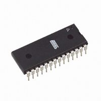
Manufacturer Part Number
ATMEGA8A-PU
Description
MCU AVR 8K FLASH 16MHZ 28-PDIP
Manufacturer
Atmel
Series
AVR® ATmegar
Specifications of ATMEGA8A-PU
Core Processor
AVR
Core Size
8-Bit
Speed
16MHz
Connectivity
I²C, SPI, UART/USART
Peripherals
Brown-out Detect/Reset, POR, PWM, WDT
Number Of I /o
23
Program Memory Size
8KB (4K x 16)
Program Memory Type
FLASH
Eeprom Size
512 x 8
Ram Size
1K x 8
Voltage - Supply (vcc/vdd)
2.7 V ~ 5.5 V
Data Converters
A/D 6x10b
Oscillator Type
Internal
Operating Temperature
-40°C ~ 85°C
Package / Case
28-DIP (0.300", 7.62mm)
Processor Series
ATMEGA8x
Core
AVR8
Data Bus Width
8 bit
Data Ram Size
1 KB
Interface Type
SPI, TWI, USART
Maximum Clock Frequency
16 MHz
Number Of Programmable I/os
23
Number Of Timers
3
Maximum Operating Temperature
+ 85 C
Mounting Style
Through Hole
3rd Party Development Tools
EWAVR, EWAVR-BL
Development Tools By Supplier
ATAVRDRAGON, ATSTK500, ATSTK600, ATAVRISP2, ATAVRONEKIT
Minimum Operating Temperature
- 40 C
On-chip Adc
10 bit, 6 Channel
Package
28PDIP
Device Core
AVR
Family Name
ATmega
Maximum Speed
16 MHz
Operating Supply Voltage
3.3|5 V
Controller Family/series
AVR MEGA
No. Of I/o's
23
Eeprom Memory Size
512Byte
Ram Memory Size
1KB
Cpu Speed
16MHz
Rohs Compliant
Yes
For Use With
ATSTK600 - DEV KIT FOR AVR/AVR32ATSTK500 - PROGRAMMER AVR STARTER KIT
Lead Free Status / RoHS Status
Lead free / RoHS Compliant
Available stocks
Company
Part Number
Manufacturer
Quantity
Price

Part Number:
ATMEGA8A-PU
Manufacturer:
ATMEL/爱特梅尔
Quantity:
20 000


22.6.2
8159D–AVR–02/11
Analog Noise Canceling Techniques
less of whether that channel is selected as input for the ADC. When the channel is selected, the
source must drive the S/H capacitor through the series resistance (combined resistance in the
input path).
The ADC is optimized for analog signals with an output impedance of approximately 10 kΩ or
less. If such a source is used, the sampling time will be negligible. If a source with higher imped-
ance is used, the sampling time will depend on how long time the source needs to charge the
S/H capacitor, with can vary widely. The user is recommended to only use low impedant sources
with slowly varying signals, since this minimizes the required charge transfer to the S/H
capacitor.
Signal components higher than the Nyquist frequency (f
kind of channels, to avoid distortion from unpredictable signal convolution. The user is advised
to remove high frequency components with a low-pass filter before applying the signals as
inputs to the ADC.
Figure 22-6. Analog Input Circuitry
Digital circuitry inside and outside the device generates EMI which might affect the accuracy of
analog measurements. If conversion accuracy is critical, the noise level can be reduced by
applying the following techniques:
1. Keep analog signal paths as short as possible. Make sure analog tracks run over the
2. The AV
3. Use the ADC noise canceler function to reduce induced noise from the CPU.
4. If any ADC [3:0] port pins are used as digital outputs, it is essential that these do not
ground plane, and keep them well away from high-speed switching digital tracks.
an LC network as shown in
switch while a conversion is in progress. However, using the Two-wire Interface (ADC4
and ADC5) will only affect the conversion on ADC4 and ADC5 and not the other ADC
channels.
ADCn
CC
pin on the device should be connected to the digital V
I
IH
Figure
I
IL
22-7.
1..100 kΩ
ADC
/2) should not be present for either
C
S/H
CC
= 14 pF
supply voltage via
ATmega8A
V
CC
/2
204
Related parts for ATMEGA8A-PU
Image
Part Number
Description
Manufacturer
Datasheet
Request
R


Part Number:
Description:
IC AVR MCU 8K 16MHZ 5V 32TQFP
Manufacturer:
Atmel
Datasheet:

Part Number:
Description:
IC AVR MCU 8K 16MHZ 5V 32-QFN
Manufacturer:
Atmel
Datasheet:

Part Number:
Description:
IC AVR MCU 8K 16MHZ 5V 28DIP
Manufacturer:
Atmel
Datasheet:
Part Number:
Description:
IC AVR MCU 8K 16MHZ COM 32-TQFP
Manufacturer:
Atmel
Datasheet:
Part Number:
Description:
IC AVR MCU 8K 16MHZ IND 32-TQFP
Manufacturer:
Atmel
Datasheet:
Part Number:
Description:
IC AVR MCU 8K 16MHZ COM 28-DIP
Manufacturer:
Atmel
Datasheet:
Part Number:
Description:
IC AVR MCU 8K 16MHZ IND 28-DIP
Manufacturer:
Atmel
Datasheet:

Part Number:
Description:
IC AVR MCU 8K 16MHZ COM 32-QFN
Manufacturer:
Atmel
Datasheet:
Part Number:
Description:
MCU AVR 8KB FLASH 16MHZ 32QFN
Manufacturer:
Atmel
Datasheet:
Part Number:
Description:
IC AVR MCU 8K 16MHZ IND 32-QFN
Manufacturer:
Atmel
Datasheet:
Part Number:
Description:
IC MCU AVR 8K 5V 16MHZ 32-TQFP
Manufacturer:
Atmel
Datasheet:
Part Number:
Description:
IC MCU AVR 8K 5V 16MHZ 32-QFN
Manufacturer:
Atmel
Datasheet:
Part Number:
Description:
IC MCU AVR 8K 5V 16MHZ 28-DIP
Manufacturer:
Atmel
Datasheet: