ATMEGA8A-PU Atmel, ATMEGA8A-PU Datasheet - Page 191
ATMEGA8A-PU
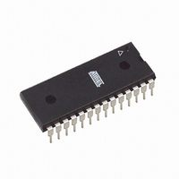
Manufacturer Part Number
ATMEGA8A-PU
Description
MCU AVR 8K FLASH 16MHZ 28-PDIP
Manufacturer
Atmel
Series
AVR® ATmegar
Specifications of ATMEGA8A-PU
Core Processor
AVR
Core Size
8-Bit
Speed
16MHz
Connectivity
I²C, SPI, UART/USART
Peripherals
Brown-out Detect/Reset, POR, PWM, WDT
Number Of I /o
23
Program Memory Size
8KB (4K x 16)
Program Memory Type
FLASH
Eeprom Size
512 x 8
Ram Size
1K x 8
Voltage - Supply (vcc/vdd)
2.7 V ~ 5.5 V
Data Converters
A/D 6x10b
Oscillator Type
Internal
Operating Temperature
-40°C ~ 85°C
Package / Case
28-DIP (0.300", 7.62mm)
Processor Series
ATMEGA8x
Core
AVR8
Data Bus Width
8 bit
Data Ram Size
1 KB
Interface Type
SPI, TWI, USART
Maximum Clock Frequency
16 MHz
Number Of Programmable I/os
23
Number Of Timers
3
Maximum Operating Temperature
+ 85 C
Mounting Style
Through Hole
3rd Party Development Tools
EWAVR, EWAVR-BL
Development Tools By Supplier
ATAVRDRAGON, ATSTK500, ATSTK600, ATAVRISP2, ATAVRONEKIT
Minimum Operating Temperature
- 40 C
On-chip Adc
10 bit, 6 Channel
Package
28PDIP
Device Core
AVR
Family Name
ATmega
Maximum Speed
16 MHz
Operating Supply Voltage
3.3|5 V
Controller Family/series
AVR MEGA
No. Of I/o's
23
Eeprom Memory Size
512Byte
Ram Memory Size
1KB
Cpu Speed
16MHz
Rohs Compliant
Yes
For Use With
ATSTK600 - DEV KIT FOR AVR/AVR32ATSTK500 - PROGRAMMER AVR STARTER KIT
Lead Free Status / RoHS Status
Lead free / RoHS Compliant
Available stocks
Company
Part Number
Manufacturer
Quantity
Price

Part Number:
ATMEGA8A-PU
Manufacturer:
ATMEL/爱特梅尔
Quantity:
20 000


20.8
20.8.1
20.8.2
8159D–AVR–02/11
Register Description
TWBR – TWI Bit Rate Register
TWCR – TWI Control Register
Figure 20-19. Possible Status Codes Caused by Arbitration
• Bits 7:0 – TWI Bit Rate Register
TWBR selects the division factor for the bit rate generator. The bit rate generator is a frequency
divider which generates the SCL clock frequency in the Master modes. See
Unit” on page 166
The TWCR is used to control the operation of the TWI. It is used to enable the TWI, to initiate a
Master access by applying a START condition to the bus, to generate a Receiver acknowledge,
to generate a stop condition, and to control halting of the bus while the data to be written to the
bus are written to the TWDR. It also indicates a write collision if data is attempted written to
TWDR while the register is inaccessible.
• Bit 7 – TWINT: TWI Interrupt Flag
This bit is set by hardware when the TWI has finished its current job and expects application
software response. If the I-bit in SREG and TWIE in TWCR are set, the MCU will jump to the
TWI Interrupt Vector. While the TWINT Flag is set, the SCL low period is stretched. The TWINT
Flag must be cleared by software by writing a logic one to it. Note that this flag is not automati-
cally cleared by hardware when executing the interrupt routine. Also note that clearing this flag
Bit
Read/Write
Initial Value
Bit
Read/Write
Initial Value
START
TWBR7
TWINT
R/W
R/W
7
0
7
0
for calculating bit rates.
Address / General Call
received
Direction
TWBR6
TWEA
Own
R/W
R/W
6
0
6
0
Yes
Arbitration lost in SLA
SLA
Write
Read
TWBR5
TWSTA
R/W
R/W
No
5
0
5
0
TWBR4
TWSTO
R/W
R/W
4
0
4
0
68/78
38
B0
Arbitration lost in Data
TWBR3
TWWC
R/W
TWI bus will be released and not addressed slave mode will be entered
A START condition will be transmitted when the bus becomes free
Data byte will be received and NOT ACK will be returned
Data byte will be received and ACK will be returned
Last data byte will be transmitted and NOT ACK should be received
Data byte will be transmitted and ACK should be received
R
3
0
3
0
Data
TWBR2
TWEN
R/W
R/W
2
0
2
0
TWBR1
R/W
R
1
0
1
–
0
ATmega8A
“Bit Rate Generator
TWBR0
TWIE
R/W
R/W
0
0
0
0
STOP
TWBR
TWCR
191
Related parts for ATMEGA8A-PU
Image
Part Number
Description
Manufacturer
Datasheet
Request
R


Part Number:
Description:
IC AVR MCU 8K 16MHZ 5V 32TQFP
Manufacturer:
Atmel
Datasheet:

Part Number:
Description:
IC AVR MCU 8K 16MHZ 5V 32-QFN
Manufacturer:
Atmel
Datasheet:

Part Number:
Description:
IC AVR MCU 8K 16MHZ 5V 28DIP
Manufacturer:
Atmel
Datasheet:
Part Number:
Description:
IC AVR MCU 8K 16MHZ COM 32-TQFP
Manufacturer:
Atmel
Datasheet:
Part Number:
Description:
IC AVR MCU 8K 16MHZ IND 32-TQFP
Manufacturer:
Atmel
Datasheet:
Part Number:
Description:
IC AVR MCU 8K 16MHZ COM 28-DIP
Manufacturer:
Atmel
Datasheet:
Part Number:
Description:
IC AVR MCU 8K 16MHZ IND 28-DIP
Manufacturer:
Atmel
Datasheet:

Part Number:
Description:
IC AVR MCU 8K 16MHZ COM 32-QFN
Manufacturer:
Atmel
Datasheet:
Part Number:
Description:
MCU AVR 8KB FLASH 16MHZ 32QFN
Manufacturer:
Atmel
Datasheet:
Part Number:
Description:
IC AVR MCU 8K 16MHZ IND 32-QFN
Manufacturer:
Atmel
Datasheet:
Part Number:
Description:
IC MCU AVR 8K 5V 16MHZ 32-TQFP
Manufacturer:
Atmel
Datasheet:
Part Number:
Description:
IC MCU AVR 8K 5V 16MHZ 32-QFN
Manufacturer:
Atmel
Datasheet:
Part Number:
Description:
IC MCU AVR 8K 5V 16MHZ 28-DIP
Manufacturer:
Atmel
Datasheet: