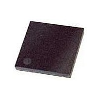
ATTINY861-15MZ Atmel, ATTINY861-15MZ Datasheet - Page 96

ATTINY861-15MZ
Manufacturer Part Number
ATTINY861-15MZ
Description
MCU AVR 8K FLASH 15MHZ 32-QFN
Manufacturer
Atmel
Series
AVR® ATtinyr
Datasheet
1.ATTINY861-15MZ.pdf
(236 pages)
Specifications of ATTINY861-15MZ
Package / Case
32-VQFN Exposed Pad, 32-HVQFN, 32-SQFN, 32-DHVQFN
Voltage - Supply (vcc/vdd)
2.7 V ~ 5.5 V
Operating Temperature
-40°C ~ 125°C
Speed
16MHz
Number Of I /o
16
Eeprom Size
512 x 8
Core Processor
AVR
Program Memory Type
FLASH
Ram Size
512 x 8
Program Memory Size
8KB (8K x 8)
Data Converters
A/D 11x10b
Oscillator Type
Internal
Peripherals
Brown-out Detect/Reset, POR, PWM, WDT
Connectivity
USI
Core Size
8-Bit
Processor Series
ATTINY8x
Core
AVR8
Data Bus Width
8 bit
Data Ram Size
512 B
Interface Type
SPI
Maximum Clock Frequency
16 MHz
Number Of Programmable I/os
16
Number Of Timers
2
Maximum Operating Temperature
+ 85 C
Mounting Style
SMD/SMT
3rd Party Development Tools
EWAVR, EWAVR-BL
Development Tools By Supplier
ATAVRDRAGON, ATSTK500, ATSTK600, ATAVRISP2, ATAVRONEKIT, ATAVRMC320
Minimum Operating Temperature
- 40 C
On-chip Adc
10 bit, 11 Channel
Lead Free Status / RoHS Status
Lead free / RoHS Compliant
Available stocks
Company
Part Number
Manufacturer
Quantity
Price
Company:
Part Number:
ATTINY861-15MZ
Manufacturer:
ATMEL
Quantity:
1 465
- Current page: 96 of 236
- Download datasheet (2Mb)
16.4
96
Output Compare Unit
ATtiny261/461/861
The comparator continuously compares TCNT1 with the Output Compare Registers (OCR1A,
OCR1B, OCR1C and OCR1D). Whenever TCNT1 equals to the Output Compare Register, the
comparator signals a match. A match will set the Output Compare Flag (OCF1A, OCF1B or
OCF1D) at the next timer clock cycle. If the corresponding interrupt is enabled, the Output Com-
pare Flag generates an Output Compare interrupt. The Output Compare Flag is automatically
cleared when the interrupt is executed. Alternatively, the flag can be cleared by software by writ-
ing a logical one to its I/O bit location. The Waveform Generator uses the match signal to
generate an output according to operating mode set by the PWM1x, WGM10 and Compare Out-
put mode (COM1x1:0) bits. The top and bottom signals are used by the Waveform Generator for
handling the special cases of the extreme values in some modes of operation
“16.7” on page
Figure 16-4. Output Compare Unit, Block Diagram
The OCR1x Registers are double buffered when using any of the Pulse Width Modulation
(PWM) modes. For the normal mode of operation, the double buffering is disabled. The double
buffering synchronizes the update of the OCR1x Compare Registers to either top or bottom of
the counting sequence. The synchronization prevents the occurrence of odd-length, non-sym-
metrical PWM pulses, thereby making the output glitch-free. See
During the time between the write and the update operation, a read from OCR1A, OCR1B,
OCR1C or OCR1D will read the contents of the temporary location. This means that the most
recently written value always will read out of OCR1A, OCR1B, OCR1C or OCR1D.
101.).
BOTTOM
FOCn
Figure 16-4
OCRnx
TOP
10-BIT OCRnx
shows a block diagram of the Output Compare unit.
Waveform Generator
=
8-BIT DATA BUS
(10-bit Comparator )
OCWnx
TCnH
10-BIT TCNTn
TCNTn
COMnX1:0
WGM10
PWMnx
Figure 16-5
OCFnx (Int.Req.)
for an example.
(See Section
2588B–AVR–11/06
Related parts for ATTINY861-15MZ
Image
Part Number
Description
Manufacturer
Datasheet
Request
R

Part Number:
Description:
Manufacturer:
Atmel Corporation
Datasheet:

Part Number:
Description:
Manufacturer:
Atmel Corporation
Datasheet:

Part Number:
Description:
IC MCU AVR 8K FLASH 20MHZ 32-QFN
Manufacturer:
Atmel
Datasheet:

Part Number:
Description:
IC MCU AVR 8K FLASH 20MHZ 20SOIC
Manufacturer:
Atmel
Datasheet:

Part Number:
Description:
MCU AVR 8K FLASH 15MHZ 20-SOIC
Manufacturer:
Atmel
Datasheet:

Part Number:
Description:
MCU AVR 8KB FLASH 15MHZ 32-VQFN
Manufacturer:
Atmel
Datasheet:

Part Number:
Description:
Microcontrollers (MCU) 8kB Flash 0.512kB EEPROM 16 I/O Pins
Manufacturer:
Atmel
Datasheet:

Part Number:
Description:
8-bit Microcontrollers - MCU 8KB FL 512B EE 512B SRAM 20MHZ IND 5V
Manufacturer:
Atmel

Part Number:
Description:
IC, MCU, 8BIT, 2K FLASH, 20SOIC
Manufacturer:
Atmel
Datasheet:

Part Number:
Description:
IC, MCU, 8BIT, 2K FLASH, 20PDIP
Manufacturer:
Atmel
Datasheet:


