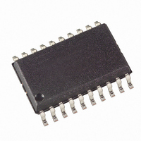
AT90PWM81-16SF Atmel, AT90PWM81-16SF Datasheet - Page 9

AT90PWM81-16SF
Manufacturer Part Number
AT90PWM81-16SF
Description
IC MCU AVR 8K FLASH ISP 20SOIC
Manufacturer
Atmel
Series
AVR® 90PWM Lightingr
Datasheet
1.AT90PWM81-16MN.pdf
(325 pages)
Specifications of AT90PWM81-16SF
Core Processor
AVR
Core Size
8-Bit
Speed
16MHz
Connectivity
SPI
Peripherals
Brown-out Detect/Reset, PWM, WDT
Number Of I /o
16
Program Memory Size
8KB (8K x 8)
Program Memory Type
FLASH
Eeprom Size
512 x 8
Ram Size
256 x 8
Voltage - Supply (vcc/vdd)
2.7 V ~ 5.5 V
Data Converters
A/D 8x10b; D/A 1x10b
Oscillator Type
Internal
Operating Temperature
-40°C ~ 105°C
Package / Case
20-SOIC (7.5mm Width)
For Use With
ATSTK600-SOIC - STK600 SOCKET/ADAPTER FOR SOIC
Lead Free Status / RoHS Status
Lead free / RoHS Compliant
Available stocks
Company
Part Number
Manufacturer
Quantity
Price
Company:
Part Number:
AT90PWM81-16SF
Manufacturer:
Atmel
Quantity:
2 428
- Current page: 9 of 325
- Download datasheet (6Mb)
3.3
3.4
7734P–AVR–08/10
ALU – Arithmetic Logic Unit
Status Register
The fast-access Register File contains 32 x 8-bit general purpose working registers with a single clock
cycle access time. This allows single-cycle Arithmetic Logic Unit (ALU) operation. In a typical ALU
operation, two operands are output from the Register File, the operation is executed, and the result is
stored back in the Register File – in one clock cycle.
Six of the 32 registers can be used as three 16-bit indirect address register pointers for Data Space address-
ing – enabling efficient address calculations. One of the these address pointers can also be used as an
address pointer for look up tables in Flash program memory. These added function registers are the 16-bit
X-, Y-, and Z-register, described later in this section.
The ALU supports arithmetic and logic operations between registers or between a constant and a register.
Single register operations can also be executed in the ALU. After an arithmetic operation, the Status Reg-
ister is updated to reflect information about the result of the operation.
Program flow is provided by conditional and unconditional jump and call instructions, able to directly
address the whole address space. Most AVR instructions have a single 16-bit word format. Every program
memory address contains a 16- or 32-bit instruction.
Program Flash memory space is divided in two sections, the Boot Program section and the Application
Program section. Both sections have dedicated Lock bits for write and read/write protection. The SPM
(Store Program Memory) instruction that writes into the Application Flash memory section must reside in
the Boot Program section.
During interrupts and subroutine calls, the return address Program Counter (PC) is stored on the Stack.
The Stack is effectively allocated in the general data SRAM, and consequently the Stack size is only lim-
ited by the total SRAM size and the usage of the SRAM. All user programs must initialize the SP in the
Reset routine (before subroutines or interrupts are executed). The Stack Pointer (SP) is read/write accessi-
ble in the I/O space. The data SRAM can easily be accessed through the five different addressing modes
supported in the AVR architecture.
The memory spaces in the AVR architecture are all linear and regular memory maps.
A flexible interrupt module has its control registers in the I/O space with an additional Global Interrupt
Enable bit in the Status Register. All interrupts have a separate Interrupt Vector in the Interrupt Vector
table. The interrupts have priority in accordance with their Interrupt Vector position. The lower the Inter-
rupt Vector address, the higher is the priority.
The I/O memory space contains 64 addresses for CPU peripheral functions as Control Registers, SPI, and
other I/O functions. The I/O Memory can be accessed directly, or as the Data Space locations following
those of the Register File, 0x20 - 0x5F. In addition, the AT90PWM81 has Extended I/O space from 0x60
- 0xFF in SRAM where only the ST/STS/STD and LD/LDS/LDD instructions can be used.
The high-performance AVR ALU operates in direct connection with all the 32 general purpose working
registers. Within a single clock cycle, arithmetic operations between general purpose registers or between
a register and an immediate are executed. The ALU operations are divided into three main categories –
arithmetic, logical, and bit-functions. Some implementations of the architecture also provide a powerful
multiplier supporting both signed/unsigned multiplication and fractional format. See the “Instruction Set”
section for a detailed description.
The Status Register contains information about the result of the most recently executed arithmetic instruc-
tion. This information can be used for altering program flow in order to perform conditional operations.
AT90PWM81
9
Related parts for AT90PWM81-16SF
Image
Part Number
Description
Manufacturer
Datasheet
Request
R

Part Number:
Description:
Manufacturer:
Atmel Corporation
Datasheet:

Part Number:
Description:
IC MCU AVR 8K FLASH ISP 20SOIC
Manufacturer:
Atmel
Datasheet:

Part Number:
Description:
IC MCU AVR 8K FLASH ISP 32QFN
Manufacturer:
Atmel
Datasheet:

Part Number:
Description:
IC MCU AVR 8K FLASH ISP 32QFN
Manufacturer:
Atmel
Datasheet:

Part Number:
Description:
8-bit Avr Microcontroller With 8k Bytes In- System Programmable Flash
Manufacturer:
ATMEL Corporation
Datasheet:

Part Number:
Description:
DEV KIT FOR AVR/AVR32
Manufacturer:
Atmel
Datasheet:

Part Number:
Description:
INTERVAL AND WIPE/WASH WIPER CONTROL IC WITH DELAY
Manufacturer:
ATMEL Corporation
Datasheet:

Part Number:
Description:
Low-Voltage Voice-Switched IC for Hands-Free Operation
Manufacturer:
ATMEL Corporation
Datasheet:

Part Number:
Description:
MONOLITHIC INTEGRATED FEATUREPHONE CIRCUIT
Manufacturer:
ATMEL Corporation
Datasheet:

Part Number:
Description:
AM-FM Receiver IC U4255BM-M
Manufacturer:
ATMEL Corporation
Datasheet:

Part Number:
Description:
Monolithic Integrated Feature Phone Circuit
Manufacturer:
ATMEL Corporation
Datasheet:

Part Number:
Description:
Multistandard Video-IF and Quasi Parallel Sound Processing
Manufacturer:
ATMEL Corporation
Datasheet:


