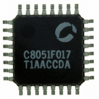
C8051F017R Silicon Laboratories Inc, C8051F017R Datasheet - Page 34

C8051F017R
Manufacturer Part Number
C8051F017R
Description
IC 8051 MCU 32K FLASH 32LQFP
Manufacturer
Silicon Laboratories Inc
Series
C8051F01xr
Specifications of C8051F017R
Core Processor
8051
Core Size
8-Bit
Speed
25MHz
Connectivity
SMBus (2-Wire/I²C), SPI, UART/USART
Peripherals
Brown-out Detect/Reset, POR, PWM, Temp Sensor, WDT
Number Of I /o
8
Program Memory Size
32KB (32K x 8)
Program Memory Type
FLASH
Ram Size
2.25K x 8
Voltage - Supply (vcc/vdd)
2.7 V ~ 3.6 V
Data Converters
A/D 4x10b; D/A 2x12b
Oscillator Type
Internal
Operating Temperature
-40°C ~ 85°C
Package / Case
32-LQFP
Lead Free Status / RoHS Status
Contains lead / RoHS non-compliant
Eeprom Size
-
Other names
336-1042-2
Q1057388
Q1057388
Available stocks
Company
Part Number
Manufacturer
Quantity
Price
Company:
Part Number:
C8051F017R
Manufacturer:
Silicon Laboratories Inc
Quantity:
10 000
- Current page: 34 of 171
- Download datasheet (2Mb)
Bit7:
Bit6:
Bit5:
Bit4:
Bits3-2: ADSTM1-0: ADC Start of Conversion Mode Bits
Bit1:
Bit0:
ADCEN
R/W
Bit7
ADCEN: ADC Enable Bit
0: ADC Disabled. ADC is in low power shutdown.
1: ADC Enabled. ADC is active and ready for data conversions.
ADCTM: ADC Track Mode Bit
0: When the ADC is enabled, tracking is always done unless a conversion is in process
1: Tracking Defined by ADSTM1-0 bits
ADCINT: ADC Conversion Complete Interrupt Flag
(Must be cleared by software)
0: ADC has not completed a data conversion since the last time this flag was cleared
1: ADC has completed a data conversion
ADBUSY: ADC Busy Bit
Read
0: ADC Conversion complete or no valid data has been converted since a reset. The falling
1: ADC Busy converting data
Write
0: No effect
1: Starts ADC Conversion if ADSTM1-0 = 00b
00: ADC conversion started upon every write of 1 to ADBUSY
01: ADC conversions taken on every overflow of Timer 3
10: ADC conversion started upon every rising edge of CNVSTR
11: ADC conversions taken on every overflow of Timer 2
ADWINT: ADC Window Compare Interrupt Flag
(Must be cleared by software)
0: ADC Window Comparison Data match has not occurred
1: ADC Window Comparison Data match occurred
ADLJST: ADC Left Justify Data Bit
0: Data in ADC0H:ADC0L Registers is right justified
1: Data in ADC0H:ADC0L Registers is left justified
edge of ADBUSY generates an interrupt when enabled.
ADCTM
R/W
Bit6
ADSTM1-0:
00: Tracking starts with the write of 1 to ADBUSY and lasts for 3 SAR clocks
01: Tracking started by the overflow of Timer 3 and last for 3 SAR clocks
10: ADC tracks only when CNVSTR input is logic low
11: Tracking started by the overflow of Timer 2 and last for 3 SAR clocks
Figure 5.7. ADC0CN: ADC Control Register (C8051F00x)
ADCINT
R/W
Bit5
ADBUSY
R/W
Bit4
Rev. 1.7
ADSTM1
R/W
Bit3
ADSTM0
R/W
Bit2
C8051F000/1/2/5/6/7
C8051F010/1/2/5/6/7
ADWINT
R/W
Bit1
(bit addressable)
ADLJST
R/W
Bit0
0xE8
SFR Address:
Reset Value
00000000
34
Related parts for C8051F017R
Image
Part Number
Description
Manufacturer
Datasheet
Request
R
Part Number:
Description:
SMD/C°/SINGLE-ENDED OUTPUT SILICON OSCILLATOR
Manufacturer:
Silicon Laboratories Inc
Part Number:
Description:
Manufacturer:
Silicon Laboratories Inc
Datasheet:
Part Number:
Description:
N/A N/A/SI4010 AES KEYFOB DEMO WITH LCD RX
Manufacturer:
Silicon Laboratories Inc
Datasheet:
Part Number:
Description:
N/A N/A/SI4010 SIMPLIFIED KEY FOB DEMO WITH LED RX
Manufacturer:
Silicon Laboratories Inc
Datasheet:
Part Number:
Description:
N/A/-40 TO 85 OC/EZLINK MODULE; F930/4432 HIGH BAND (REV E/B1)
Manufacturer:
Silicon Laboratories Inc
Part Number:
Description:
EZLink Module; F930/4432 Low Band (rev e/B1)
Manufacturer:
Silicon Laboratories Inc
Part Number:
Description:
I°/4460 10 DBM RADIO TEST CARD 434 MHZ
Manufacturer:
Silicon Laboratories Inc
Part Number:
Description:
I°/4461 14 DBM RADIO TEST CARD 868 MHZ
Manufacturer:
Silicon Laboratories Inc
Part Number:
Description:
I°/4463 20 DBM RFSWITCH RADIO TEST CARD 460 MHZ
Manufacturer:
Silicon Laboratories Inc
Part Number:
Description:
I°/4463 20 DBM RADIO TEST CARD 868 MHZ
Manufacturer:
Silicon Laboratories Inc
Part Number:
Description:
I°/4463 27 DBM RADIO TEST CARD 868 MHZ
Manufacturer:
Silicon Laboratories Inc
Part Number:
Description:
I°/4463 SKYWORKS 30 DBM RADIO TEST CARD 915 MHZ
Manufacturer:
Silicon Laboratories Inc
Part Number:
Description:
N/A N/A/-40 TO 85 OC/4463 RFMD 30 DBM RADIO TEST CARD 915 MHZ
Manufacturer:
Silicon Laboratories Inc
Part Number:
Description:
I°/4463 20 DBM RADIO TEST CARD 169 MHZ
Manufacturer:
Silicon Laboratories Inc


