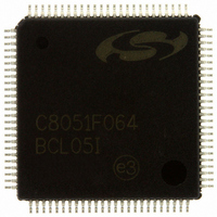
C8051F064-GQ Silicon Laboratories Inc, C8051F064-GQ Datasheet - Page 238

C8051F064-GQ
Manufacturer Part Number
C8051F064-GQ
Description
IC 8051 MCU 64K FLASH 100TQFP
Manufacturer
Silicon Laboratories Inc
Series
C8051F06xr
Specifications of C8051F064-GQ
Program Memory Type
FLASH
Program Memory Size
64KB (64K x 8)
Package / Case
100-TQFP, 100-VQFP
Core Processor
8051
Core Size
8-Bit
Speed
25MHz
Connectivity
EBI/EMI, SMBus (2-Wire/I²C), SPI, UART/USART
Peripherals
Brown-out Detect/Reset, POR, PWM, WDT
Number Of I /o
59
Ram Size
4.25K x 8
Voltage - Supply (vcc/vdd)
2.7 V ~ 3.6 V
Data Converters
A/D 2x16b
Oscillator Type
Internal
Operating Temperature
-40°C ~ 85°C
Processor Series
C8051F0x
Core
8051
Data Bus Width
8 bit
Data Ram Size
4.25 KB
Interface Type
I2C, SMBus, SPI, UART
Maximum Clock Frequency
25 MHz
Number Of Programmable I/os
59
Number Of Timers
5
Operating Supply Voltage
2.7 V to 3.6 V
Maximum Operating Temperature
+ 85 C
Mounting Style
SMD/SMT
3rd Party Development Tools
PK51, CA51, A51, ULINK2
Development Tools By Supplier
C8051F060DK
Minimum Operating Temperature
- 40 C
On-chip Adc
16 bit, 1 Channel
On-chip Dac
12 bit, 2 Channel
No. Of I/o's
59
Ram Memory Size
4352Byte
Cpu Speed
25MHz
No. Of Timers
5
Rohs Compliant
Yes
Package
100TQFP
Device Core
8051
Family Name
C8051F06x
Maximum Speed
25 MHz
Data Rom Size
64 KB
A/d Bit Size
16 bit
A/d Channels Available
1
Height
1.05 mm
Length
14 mm
Supply Voltage (max)
3.6 V
Supply Voltage (min)
2.7 V
Width
14 mm
Lead Free Status / RoHS Status
Lead free / RoHS Compliant
For Use With
336-1219 - KIT EVAL FOR C8051F064
Eeprom Size
-
Lead Free Status / Rohs Status
Lead free / RoHS Compliant
Other names
336-1218
Available stocks
Company
Part Number
Manufacturer
Quantity
Price
Company:
Part Number:
C8051F064-GQ
Manufacturer:
SiliconL
Quantity:
28
Company:
Part Number:
C8051F064-GQ
Manufacturer:
Silicon Laboratories Inc
Quantity:
10 000
Company:
Part Number:
C8051F064-GQR
Manufacturer:
Silicon Laboratories Inc
Quantity:
10 000
Part Number:
C8051F064-GQR
Manufacturer:
SILICONLABS/芯科
Quantity:
20 000
C8051F060/1/2/3/4/5/6/7
20.3. SMBus Transfer Modes
The SMBus0 interface may be configured to operate as a master and/or a slave. At any particular time, the
interface will be operating in one of the following modes: Master Transmitter, Master Receiver, Slave
Transmitter, or Slave Receiver. See Table 20.1 for transfer mode status decoding using the SMB0STA sta-
tus register. The following mode descriptions illustrate an interrupt-driven SMBus0 application; SMBus0
may alternatively be operated in polled mode.
20.3.1. Master Transmitter Mode
Serial data is transmitted on SDA while the serial clock is output on SCL. SMBus0 generates a START
condition and then transmits the first byte containing the address of the target slave device and the data
direction bit. In this case the data direction bit (R/W) will be logic 0 to indicate a "WRITE" operation. The
SMBus0 interface transmits one or more bytes of serial data, waiting for an acknowledge (ACK) from the
slave after each byte. To indicate the end of the serial transfer, SMBus0 generates a STOP condition.
20.3.2. Master Receiver Mode
Serial data is received on SDA while the serial clock is output on SCL. The SMBus0 interface generates a
START followed by the first data byte containing the address of the target slave and the data direction bit.
In this case the data direction bit (R/W) will be logic 1 to indicate a "READ" operation. The SMBus0 inter-
face receives serial data from the slave and generates the clock on SCL. After each byte is received,
SMBus0 generates an ACK or NACK depending on the state of the AA bit in register SMB0CN. SMBus0
generates a STOP condition to indicate the end of the serial transfer.
238
Interrupt
S
Interrupt
S
Received by SMBus
Interface
Transmitted by
SMBus Interface
Received by SMBus
Interface
Transmitted by
SMBus Interface
SLA
SLA
Figure 20.4. Typical Master Transmitter Sequence
Figure 20.5. Typical Master Receiver Sequence
W
R
Interrupt
A
Interrupt
A
Data Byte
Data Byte
Rev. 1.2
Interrupt
Interrupt
A
A
S = START
P = STOP
A = ACK
N = NACK
R = READ
SLA = Slave Address
Data Byte
S = START
P = STOP
A = ACK
W = WRITE
SLA = Slave Address
Data Byte
Interrupt
N
Interrupt
A
P
P


