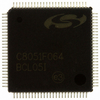
C8051F064-GQ Silicon Laboratories Inc, C8051F064-GQ Datasheet - Page 208

C8051F064-GQ
Manufacturer Part Number
C8051F064-GQ
Description
IC 8051 MCU 64K FLASH 100TQFP
Manufacturer
Silicon Laboratories Inc
Series
C8051F06xr
Specifications of C8051F064-GQ
Program Memory Type
FLASH
Program Memory Size
64KB (64K x 8)
Package / Case
100-TQFP, 100-VQFP
Core Processor
8051
Core Size
8-Bit
Speed
25MHz
Connectivity
EBI/EMI, SMBus (2-Wire/I²C), SPI, UART/USART
Peripherals
Brown-out Detect/Reset, POR, PWM, WDT
Number Of I /o
59
Ram Size
4.25K x 8
Voltage - Supply (vcc/vdd)
2.7 V ~ 3.6 V
Data Converters
A/D 2x16b
Oscillator Type
Internal
Operating Temperature
-40°C ~ 85°C
Processor Series
C8051F0x
Core
8051
Data Bus Width
8 bit
Data Ram Size
4.25 KB
Interface Type
I2C, SMBus, SPI, UART
Maximum Clock Frequency
25 MHz
Number Of Programmable I/os
59
Number Of Timers
5
Operating Supply Voltage
2.7 V to 3.6 V
Maximum Operating Temperature
+ 85 C
Mounting Style
SMD/SMT
3rd Party Development Tools
PK51, CA51, A51, ULINK2
Development Tools By Supplier
C8051F060DK
Minimum Operating Temperature
- 40 C
On-chip Adc
16 bit, 1 Channel
On-chip Dac
12 bit, 2 Channel
No. Of I/o's
59
Ram Memory Size
4352Byte
Cpu Speed
25MHz
No. Of Timers
5
Rohs Compliant
Yes
Package
100TQFP
Device Core
8051
Family Name
C8051F06x
Maximum Speed
25 MHz
Data Rom Size
64 KB
A/d Bit Size
16 bit
A/d Channels Available
1
Height
1.05 mm
Length
14 mm
Supply Voltage (max)
3.6 V
Supply Voltage (min)
2.7 V
Width
14 mm
Lead Free Status / RoHS Status
Lead free / RoHS Compliant
For Use With
336-1219 - KIT EVAL FOR C8051F064
Eeprom Size
-
Lead Free Status / Rohs Status
Lead free / RoHS Compliant
Other names
336-1218
Available stocks
Company
Part Number
Manufacturer
Quantity
Price
Company:
Part Number:
C8051F064-GQ
Manufacturer:
SiliconL
Quantity:
28
Company:
Part Number:
C8051F064-GQ
Manufacturer:
Silicon Laboratories Inc
Quantity:
10 000
Company:
Part Number:
C8051F064-GQR
Manufacturer:
Silicon Laboratories Inc
Quantity:
10 000
Part Number:
C8051F064-GQR
Manufacturer:
SILICONLABS/芯科
Quantity:
20 000
- Current page: 208 of 328
- Download datasheet (2Mb)
C8051F060/1/2/3/4/5/6/7
18.1.6. Crossbar Pin Assignment Example
In this example (Figure 18.4), we configure the Crossbar to allocate Port pins for UART0, the SMBus, all 6
PCA modules, /INT0, and /INT1 (12 pins total). Additionally, we configure P1.2, P1.3, and P1.4 for Analog
Input mode so that the voltages at these pins can be measured by ADC2. The configuration steps are as
follows:
XBR0, XBR1, and XBR2 are set such that UART0EN = 1, SMB0EN = 1, PCA0ME = ‘110’, INT0E = 1, and
INT1E = 1. Thus: XBR0 = 0x3D, XBR1 = 0x14, and XBR2 = 0x40.
208
1. We configure the desired Port 1 pins to Analog Input mode by setting P1MDIN to 0xE3 (P1.4,
2. We enable the Crossbar by setting XBARE = 1: XBR2 = 0x40.
3. We set the UART0 TX pin (TX0, P0.0) output and the CEX0-3 outputs to Push-Pull by setting
4. We explicitly disable the output drivers on the 3 Analog Input pins by setting the corresponding
P1.3, and P1.2 are Analog Inputs, so their associated P1MDIN bits are set to logic 0).
-
-
-
-
-
-
P0MDOUT = 0xF1.
bits in the P1MDOUT register to ‘0’, and in P1 to ‘1’. Additionally, the CEX5-4 output pins are
set to Push-Pull mode. Therefore, P1MDOUT = 0x03 (configure unused pins to Open-Drain)
and P1 = 0xFF (a logic 1 selects the high-impedance state).
UART0 has the highest priority, so P0.0 is assigned to TX0, and P0.1 is assigned to RX0.
The SMBus is next in priority order, so P0.2 is assigned to SDA, and P0.3 is assigned to
SCL.
PCA0 is next in priority order, so P0.4 through P1.1 are assigned to CEX0 through CEX5
P1MDIN is set to 0xE3, which configures P1.2, P1.3, and P1.4 as Analog Inputs, causing
the Crossbar to skip these pins.
/INT0 is next in priority order, so it is assigned to the next non-skipped pin, which is P1.5.
/INT1 is next in priority order, so it is assigned to P1.6.
Rev. 1.2
Related parts for C8051F064-GQ
Image
Part Number
Description
Manufacturer
Datasheet
Request
R
Part Number:
Description:
SMD/C°/SINGLE-ENDED OUTPUT SILICON OSCILLATOR
Manufacturer:
Silicon Laboratories Inc
Part Number:
Description:
Manufacturer:
Silicon Laboratories Inc
Datasheet:
Part Number:
Description:
N/A N/A/SI4010 AES KEYFOB DEMO WITH LCD RX
Manufacturer:
Silicon Laboratories Inc
Datasheet:
Part Number:
Description:
N/A N/A/SI4010 SIMPLIFIED KEY FOB DEMO WITH LED RX
Manufacturer:
Silicon Laboratories Inc
Datasheet:
Part Number:
Description:
N/A/-40 TO 85 OC/EZLINK MODULE; F930/4432 HIGH BAND (REV E/B1)
Manufacturer:
Silicon Laboratories Inc
Part Number:
Description:
EZLink Module; F930/4432 Low Band (rev e/B1)
Manufacturer:
Silicon Laboratories Inc
Part Number:
Description:
I°/4460 10 DBM RADIO TEST CARD 434 MHZ
Manufacturer:
Silicon Laboratories Inc
Part Number:
Description:
I°/4461 14 DBM RADIO TEST CARD 868 MHZ
Manufacturer:
Silicon Laboratories Inc
Part Number:
Description:
I°/4463 20 DBM RFSWITCH RADIO TEST CARD 460 MHZ
Manufacturer:
Silicon Laboratories Inc
Part Number:
Description:
I°/4463 20 DBM RADIO TEST CARD 868 MHZ
Manufacturer:
Silicon Laboratories Inc
Part Number:
Description:
I°/4463 27 DBM RADIO TEST CARD 868 MHZ
Manufacturer:
Silicon Laboratories Inc
Part Number:
Description:
I°/4463 SKYWORKS 30 DBM RADIO TEST CARD 915 MHZ
Manufacturer:
Silicon Laboratories Inc
Part Number:
Description:
N/A N/A/-40 TO 85 OC/4463 RFMD 30 DBM RADIO TEST CARD 915 MHZ
Manufacturer:
Silicon Laboratories Inc
Part Number:
Description:
I°/4463 20 DBM RADIO TEST CARD 169 MHZ
Manufacturer:
Silicon Laboratories Inc


