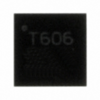
C8051T606-GM Silicon Laboratories Inc, C8051T606-GM Datasheet - Page 17

C8051T606-GM
Manufacturer Part Number
C8051T606-GM
Description
IC 8051 MCU 1.5K-EEPROM 11-QFN
Manufacturer
Silicon Laboratories Inc
Series
C8051T60xr
Specifications of C8051T606-GM
Program Memory Type
OTP
Program Memory Size
1.5KB (1.5K x 8)
Package / Case
11-QFN
Core Processor
8051
Core Size
8-Bit
Speed
25MHz
Connectivity
SMBus (2-Wire/I²C), UART/USART
Peripherals
POR, PWM, WDT
Number Of I /o
6
Ram Size
128 x 8
Voltage - Supply (vcc/vdd)
1.8 V ~ 3.6 V
Oscillator Type
Internal
Operating Temperature
-40°C ~ 85°C
Processor Series
C8051T6x
Core
8051
Data Bus Width
8 bit
Data Ram Size
128 B
Interface Type
I2C, UART
Maximum Clock Frequency
25 MHz
Number Of Programmable I/os
6
Number Of Timers
3
Operating Supply Voltage
1.8 V to 3.6 V
Maximum Operating Temperature
+ 85 C
Mounting Style
SMD/SMT
3rd Party Development Tools
PK51, CA51, A51, ULINK2
Development Tools By Supplier
C8051T606DK
Minimum Operating Temperature
- 40 C
Package
11QFN EP
Device Core
8051
Family Name
C8051T60x
Maximum Speed
25 MHz
Lead Free Status / RoHS Status
Lead free / RoHS Compliant
For Use With
336-1668 - CARD DAUGHTER QFN10 SOCKET336-1667 - CARD DAUGHTER MSOP SOCKET336-1666 - KIT DEVELOPMENT FOR C8051T606336-1404 - KIT DEV FOR C8051T60X MCU'S
Eeprom Size
-
Data Converters
-
Lead Free Status / Rohs Status
Lead free / RoHS Compliant
Other names
336-1662-5
Available stocks
Company
Part Number
Manufacturer
Quantity
Price
Company:
Part Number:
C8051T606-GM
Manufacturer:
SILICON
Quantity:
3 500
Part Number:
C8051T606-GM
Manufacturer:
SILICONLABS/芯科
Quantity:
20 000
3. Pin Definitions
Table 3.1. Pin Definitions for the C8051T600/1/2/3/4/5
CNVSTR
EXTCLK
Name
C2CK
P0.7 /
P0.0 /
VREF
P0.2 /
P0.3 /
P0.6 /
RST /
GND
P0.4
P0.5
C2D
P0.1
V
V
NC
DD
PP
QFN11
Pin
10
11
—
3
8
1
2
4
5
6
7
9
SOIC14
4,9,11
Pin
14
10
12
13
7
3
2
5
6
8
1
D I/O or
D I/O or
D I/O or
D I/O or
D I/O or
D I/O or
D I/O or
D I/O or
A I/O or
D I/O
D I/O
D I/O
Type
D In
D In
A In
A In
A In
A In
A In
A In
A In
A In
A In
A In
Description
Power Supply Voltage.
Ground.
Device Reset. Open-drain output of internal POR or V
Clock signal for the C2 Debug Interface.
Port 0.7.
Bi-directional data signal for the C2 Debug Interface.
Port 0.0.
External VREF input.
Port 0.1.
Port 0.2.
V
Port 0.3.
External Clock Pin. This pin can be used as the external clock
input for CMOS, capacitor, or RC oscillator configurations.
Port 0.4.
Port 0.5.
Port 0.6.
ADC0 External Convert Start Input.
No Connection.
PP
Programming Supply Voltage.
Rev. 1.2
C8051T600/1/2/3/4/5/6
DD
monitor.
17


