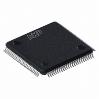
LPC2158FBD100,551 NXP Semiconductors, LPC2158FBD100,551 Datasheet - Page 17

LPC2158FBD100,551
Manufacturer Part Number
LPC2158FBD100,551
Description
IC ARM7 MCU FLASH 512K 100LQFP
Manufacturer
NXP Semiconductors
Series
LPC2100r
Datasheet
1.LPC2157FBD100551.pdf
(45 pages)
Specifications of LPC2158FBD100,551
Core Processor
ARM7
Core Size
16/32-Bit
Speed
60MHz
Connectivity
I²C, Microwire, SPI, SSI, SSP, UART/USART, USB
Peripherals
Brown-out Detect/Reset, DMA, LCD, POR, PWM, WDT
Number Of I /o
38
Program Memory Size
512KB (512K x 8)
Program Memory Type
FLASH
Ram Size
40K x 8
Voltage - Supply (vcc/vdd)
3 V ~ 3.6 V
Data Converters
A/D 14x10b; D/A 1x10b
Oscillator Type
Internal
Operating Temperature
-40°C ~ 85°C
Package / Case
100-LQFP
Processor Series
LPC21
Core
ARM7TDMI-S
Data Bus Width
32 bit
Data Ram Size
40 KB
Interface Type
I2C, SPI
Maximum Clock Frequency
25 MHz
Number Of Programmable I/os
38
Number Of Timers
2
Operating Supply Voltage
2.4 V to 3.6 V
Maximum Operating Temperature
+ 85 C
Mounting Style
SMD/SMT
3rd Party Development Tools
MDK-ARM, RL-ARM, ULINK2, LCD-DEMO-LPC2158
Development Tools By Supplier
OM11020
Minimum Operating Temperature
- 40 C
On-chip Adc
10 bit, 8 Channel
On-chip Dac
10 bit, 1 Channel
For Use With
568-4310 - EVAL BOARD LPC2158 W/LCD568-4297 - BOARD EVAL LPC21XX MCB2100622-1005 - USB IN-CIRCUIT PROG ARM7 LPC2K
Lead Free Status / RoHS Status
Lead free / RoHS Compliant
Eeprom Size
-
Lead Free Status / Rohs Status
Details
Other names
568-4691
935287349551
LPC2158FBD100-S
935287349551
LPC2158FBD100-S
Available stocks
Company
Part Number
Manufacturer
Quantity
Price
Company:
Part Number:
LPC2158FBD100,551
Manufacturer:
NXP Semiconductors
Quantity:
10 000
NXP Semiconductors
LPC2157_2158_1
Product data sheet
6.5.1 Interrupt sources
6.6 Pin connect block
6.7 Fast general purpose parallel I/O
FIQ has the highest priority. If more than one request is assigned to FIQ, the VIC
combines the requests to produce the FIQ signal to the ARM processor. The fastest
possible FIQ latency is achieved when only one request is classified as FIQ, because then
the FIQ service routine does not need to branch into the interrupt service routine but can
run from the interrupt vector location. If more than one request is assigned to the FIQ
class, the FIQ service routine will read a word from the VIC that identifies which FIQ
source(s) is (are) requesting an interrupt.
Vectored IRQs have the middle priority. Sixteen of the interrupt requests can be assigned
to this category. Any of the interrupt requests can be assigned to any of the 16 vectored
IRQ slots, among which slot 0 has the highest priority and slot 15 has the lowest.
Non-vectored IRQs have the lowest priority.
The VIC combines the requests from all the vectored and non-vectored IRQs to produce
the IRQ signal to the ARM processor. The IRQ service routine can start by reading a
register from the VIC and jumping there. If any of the vectored IRQs are pending, the VIC
provides the address of the highest-priority requesting IRQs service routine, otherwise it
provides the address of a default routine that is shared by all the non-vectored IRQs. The
default routine can read another VIC register to see what IRQs are active.
Each peripheral device has one interrupt line connected to the Vectored Interrupt
Controller, but may have several internal interrupt flags. Individual interrupt flags may also
represent more than one interrupt source.
The pin connect block allows selected pins of the microcontroller to have more than one
function. Configuration registers control the multiplexers to allow connection between the
pin and the on chip peripherals. Peripherals should be connected to the appropriate pins
prior to being activated, and prior to any related interrupt(s) being enabled. Activity of any
enabled peripheral function that is not mapped to a related pin should be considered
undefined.
The Pin Control Module with its pin select registers defines the functionality of the
microcontroller in a given hardware environment.
After reset all pins of Port 0 and Port 1 are configured as input with the following
exceptions: If debug is enabled, the JTAG pins will assume their JTAG functionality. The
pins associated with the I
Device pins that are not connected to a specific peripheral function are controlled by the
GPIO registers. Pins may be dynamically configured as inputs or outputs. Separate
registers allow setting or clearing any number of outputs simultaneously. The value of the
output register may be read back, as well as the current state of the port pins.
LPC2157/2158 introduce accelerated GPIO functions over prior LPC2000 devices:
•
GPIO registers are relocated to the ARM local bus for the fastest possible I/O timing.
Rev. 01 — 15 October 2008
2
C0 and I
2
C1 interface are open drain.
Single-chip 16-bit/32-bit microcontrollers
LPC2157/2158
© NXP B.V. 2008. All rights reserved.
17 of 45


