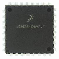
MC9S12H128VFVE Freescale Semiconductor, MC9S12H128VFVE Datasheet - Page 65

MC9S12H128VFVE
Manufacturer Part Number
MC9S12H128VFVE
Description
IC MCU 128K FLASH 16MHZ 144-LQFP
Manufacturer
Freescale Semiconductor
Series
HCS12r
Datasheet
1.MC9S12H256VFVER.pdf
(130 pages)
Specifications of MC9S12H128VFVE
Core Processor
HCS12
Core Size
16-Bit
Speed
16MHz
Connectivity
CAN, I²C, SCI, SPI
Peripherals
LCD, POR, PWM, WDT
Number Of I /o
99
Program Memory Size
128KB (128K x 8)
Program Memory Type
FLASH
Eeprom Size
4K x 8
Ram Size
6K x 8
Voltage - Supply (vcc/vdd)
2.35 V ~ 5.25 V
Data Converters
A/D 8x10b
Oscillator Type
Internal
Operating Temperature
-40°C ~ 105°C
Package / Case
144-LQFP
Processor Series
S12H
Core
HCS12
Data Bus Width
16 bit
Data Ram Size
6 KB
Interface Type
CAN/I2C/SCI/SPI
Maximum Clock Frequency
16 MHz
Number Of Programmable I/os
99
Number Of Timers
8
Operating Supply Voltage
- 0.3 V to + 6 V
Maximum Operating Temperature
+ 105 C
Mounting Style
SMD/SMT
3rd Party Development Tools
EWHCS12
Minimum Operating Temperature
- 40 C
On-chip Adc
16-ch x 10-bit
Package
144LQFP
Family Name
HCS12
Maximum Speed
16 MHz
Lead Free Status / RoHS Status
Lead free / RoHS Compliant
Available stocks
Company
Part Number
Manufacturer
Quantity
Price
Company:
Part Number:
MC9S12H128VFVE
Manufacturer:
Freescale Semiconductor
Quantity:
10 000
MC9S12H256 Device User Guide — V01.20
2.3.38 PS1 / TXD0 — Port S I/O Pin 1
PS1 is a general purpose input or output pin. It can be configured as transmit pin TXD0 of the Serial
Communication Interface 0 (SCI0).
2.3.39 PS0 / RXD0 — Port S I/O Pin 0
PS0 is a general purpose input or output pin. It can be configured as receive pin RXD0 of the Serial
Communication Interface 0 (SCI0).
2.3.40 PT[7:4] / IOC[7:4] — Port T I/O Pins [7:4]
PT7-PT4 are general purpose input or output pins. They can be configured as input capture or output
compare pins IOC7-IOC4 of the Timer (TIM).
2.3.41 PT[3:0] / IOC[3:0] / FP[27:24] — Port T I/O Pins [3:0]
PT3-PT0 are general purpose input or output pins. They can be configured as input capture or output
compare pins IOC3-IOC0 of the Timer (TIM). They can be configured as frontplane segment driver
outputs FP27-FP24 of the LCD module.
2.3.42 PU[7:4] / M1C1P, M1C1M, M1C0P, M1C0M — Port U I/O Pins [7:4]
PU7-PU4 are general purpose input or output pins. They can be configured as high current PWM output
pins which can be used for motor drive. These pins interface to the coils of motor 1. PWM output on
M1C0M results in a positive current flow through coil 0 when M1C0P is driven to a logic high state. PWM
output on M1C1M results in a positive current flow through coil 1 when M1C1P is driven to a logic high
state.
2.3.43 PU[3:0] / M0C1P, M0C1M, M0C0P, M0C0M — Port U I/O Pins [3:0]
PU3-PU0 are general purpose input or output pins. They can be configured as high current PWM output
pins which can be used for motor drive. These pins interface to the coils of motor 0. PWM output on
M0C0M results in a positive current flow through coil 0 when M0C0P is driven to a logic high state. PWM
output on M0C1M results in a positive current flow through coil 1 when M0C1P is driven to a logic high
state.
2.3.44 PV[7:4] / M3C1P, M3C1M, M3C0P, M3C0M — Port V I/O Pins [7:4]
PV7-PV4 are general purpose input or output pins. They can be configured as high current PWM output
pins which can be used for motor drive. These pins interface to the coils of motor 3. PWM output on
M3C0M results in a positive current flow through coil 0 when M3C0P is driven to a logic high state. PWM
output on M3C1M results in a positive current flow through coil 1 when M3C1P is driven to a logic high
state.
65


