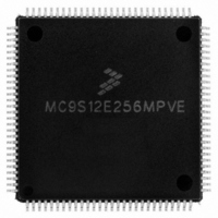
MC9S12E256MPVE Freescale Semiconductor, MC9S12E256MPVE Datasheet - Page 77

MC9S12E256MPVE
Manufacturer Part Number
MC9S12E256MPVE
Description
IC MCU 256K FLASH 25MHZ 112-LQFP
Manufacturer
Freescale Semiconductor
Series
HCS12r
Specifications of MC9S12E256MPVE
Core Processor
HCS12
Core Size
16-Bit
Speed
25MHz
Connectivity
EBI/EMI, I²C, SCI, SPI
Peripherals
POR, PWM, WDT
Number Of I /o
91
Program Memory Size
256KB (256K x 8)
Program Memory Type
FLASH
Ram Size
16K x 8
Voltage - Supply (vcc/vdd)
2.35 V ~ 2.75 V
Data Converters
A/D 16x10b; D/A 2x8b
Oscillator Type
Internal
Operating Temperature
-40°C ~ 125°C
Package / Case
112-LQFP
Processor Series
S12E
Core
HCS12
Data Bus Width
16 bit
Data Ram Size
16 KB
Interface Type
I2C/SCI/SPI
Maximum Clock Frequency
50 MHz
Number Of Programmable I/os
92
Number Of Timers
12
Operating Supply Voltage
0 V to 5 V
Maximum Operating Temperature
+ 125 C
Mounting Style
SMD/SMT
3rd Party Development Tools
EWHCS12
Minimum Operating Temperature
- 40 C
On-chip Adc
16-ch x 10-bit
On-chip Dac
2-ch x 8-bit
For Use With
M68EVB912E128 - BOARD EVAL FOR MC9S12E128/64
Lead Free Status / RoHS Status
Lead free / RoHS Compliant
Eeprom Size
-
Lead Free Status / Rohs Status
Lead free / RoHS Compliant
Available stocks
Company
Part Number
Manufacturer
Quantity
Price
Company:
Part Number:
MC9S12E256MPVE
Manufacturer:
Freescale Semiconductor
Quantity:
10 000
- Current page: 77 of 602
- Download datasheet (4Mb)
1.9.2.2
When a reset occurs, MCU registers and control bits are changed to known start-up states. Refer to the
respective module block description chapters for register reset states. Refer to
External Bus Interface (MEBIV3)”
Refer to
module ports.
Refer to
The RAM array is not automatically initialized out of reset.
1.10
The Printed Circuit Board (PCB) must be carefully laid out to ensure proper operation of the voltage
regulator as well as the MCU itself. The following rules must be observed:
Freescale Semiconductor
•
•
•
•
•
•
•
Every supply pair must be decoupled by a ceramic capacitor connected as near as possible to the
corresponding pins (C1–C6).
Central point of the ground star should be the VSSR pin.
Use low ohmic low inductance connections between VSS1, VSS2 and VSSR.
VSSPLL must be directly connected to VSSR.
Keep traces of VSSPLL, EXTAL and XTAL as short as possible and occupied board area for C7,
C8, C11 and Q1 as small as possible.
Do not place other signals or supplies underneath area occupied by C7, C8, C10 and Q1 and the
connection area to the MCU.
Central power input should be fed in at the VDDA/VSSA pins.
Chapter 3, “Port Integration Module (PIM9E256V1)”
Table 1-1
Recommended Printed Circuit Board Layout
Effects of Reset
Component
for locations of the memories depending on the operating mode after reset.
C10
C11
Q1
C1
C2
C3
C4
C5
C6
C7
C8
C9
R1
Table 1-11. Recommended Decoupling Capacitor Choice
VDD2 filter cap (80 QFP only)
VDDPLL filter cap
PLL loop filter cap
PLL loop filter cap
PLL loop filter res
VDDR filter cap
VDD1 filter cap
VDDA filter cap
VDDX filter cap
for mode dependent pin configuration of port A, B and E out of reset.
OSC load cap
OSC load cap
DC cutoff cap
MC9S12E256 Data Sheet, Rev. 1.08
Purpose
Quartz
Chapter 1 MC9S12E256 Device Overview (MC9S12E256DGV1)
X7R/tantalum
X7R/tantalum
Ceramic X7R
Ceramic X7R
Ceramic X7R
Ceramic X7R
See PLL specification chapter
Type
for reset configurations of all peripheral
100–220nF
100–220nF
Chapter 18, “Multiplexed
>=100nF
>=100nF
100nF
100nF
Value
77
Related parts for MC9S12E256MPVE
Image
Part Number
Description
Manufacturer
Datasheet
Request
R
Part Number:
Description:
Manufacturer:
Freescale Semiconductor, Inc
Datasheet:
Part Number:
Description:
Manufacturer:
Freescale Semiconductor, Inc
Datasheet:
Part Number:
Description:
Manufacturer:
Freescale Semiconductor, Inc
Datasheet:
Part Number:
Description:
Manufacturer:
Freescale Semiconductor, Inc
Datasheet:
Part Number:
Description:
Manufacturer:
Freescale Semiconductor, Inc
Datasheet:
Part Number:
Description:
Manufacturer:
Freescale Semiconductor, Inc
Datasheet:
Part Number:
Description:
Manufacturer:
Freescale Semiconductor, Inc
Datasheet:
Part Number:
Description:
Manufacturer:
Freescale Semiconductor, Inc
Datasheet:
Part Number:
Description:
Manufacturer:
Freescale Semiconductor, Inc
Datasheet:
Part Number:
Description:
Manufacturer:
Freescale Semiconductor, Inc
Datasheet:
Part Number:
Description:
Manufacturer:
Freescale Semiconductor, Inc
Datasheet:
Part Number:
Description:
Manufacturer:
Freescale Semiconductor, Inc
Datasheet:
Part Number:
Description:
Manufacturer:
Freescale Semiconductor, Inc
Datasheet:
Part Number:
Description:
Manufacturer:
Freescale Semiconductor, Inc
Datasheet:
Part Number:
Description:
Manufacturer:
Freescale Semiconductor, Inc
Datasheet:


