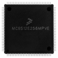
MC9S12E256MPVE Freescale Semiconductor, MC9S12E256MPVE Datasheet - Page 69

MC9S12E256MPVE
Manufacturer Part Number
MC9S12E256MPVE
Description
IC MCU 256K FLASH 25MHZ 112-LQFP
Manufacturer
Freescale Semiconductor
Series
HCS12r
Specifications of MC9S12E256MPVE
Core Processor
HCS12
Core Size
16-Bit
Speed
25MHz
Connectivity
EBI/EMI, I²C, SCI, SPI
Peripherals
POR, PWM, WDT
Number Of I /o
91
Program Memory Size
256KB (256K x 8)
Program Memory Type
FLASH
Ram Size
16K x 8
Voltage - Supply (vcc/vdd)
2.35 V ~ 2.75 V
Data Converters
A/D 16x10b; D/A 2x8b
Oscillator Type
Internal
Operating Temperature
-40°C ~ 125°C
Package / Case
112-LQFP
Processor Series
S12E
Core
HCS12
Data Bus Width
16 bit
Data Ram Size
16 KB
Interface Type
I2C/SCI/SPI
Maximum Clock Frequency
50 MHz
Number Of Programmable I/os
92
Number Of Timers
12
Operating Supply Voltage
0 V to 5 V
Maximum Operating Temperature
+ 125 C
Mounting Style
SMD/SMT
3rd Party Development Tools
EWHCS12
Minimum Operating Temperature
- 40 C
On-chip Adc
16-ch x 10-bit
On-chip Dac
2-ch x 8-bit
For Use With
M68EVB912E128 - BOARD EVAL FOR MC9S12E128/64
Lead Free Status / RoHS Status
Lead free / RoHS Compliant
Eeprom Size
-
Lead Free Status / Rohs Status
Lead free / RoHS Compliant
Available stocks
Company
Part Number
Manufacturer
Quantity
Price
Company:
Part Number:
MC9S12E256MPVE
Manufacturer:
Freescale Semiconductor
Quantity:
10 000
- Current page: 69 of 602
- Download datasheet (4Mb)
function is selected. While in reset and immediately out of reset the PU[3:0] pins are configured as a high
impedance input pins. Consult
Module
about pin configurations.
1.4.43
External power and ground for I/O drivers. Bypass requirements depend on how heavily the MCU pins are
loaded.
1.4.44
External power and ground for I/O drivers and input to the internal voltage regulator. Bypass requirements
depend on how heavily the MCU pins are loaded.
1.4.45
Power is supplied to the MCU through VDD and VSS. This 2.5V supply is derived from the internal
voltage regulator. There is no static load on those pins allowed. The internal voltage regulator is turned off,
if VDDR is tied to ground.
1.4.46
VDDA, VSSA are the power supply and ground input pins for the voltage regulator and the analog to
digital converter.
1.4.47
VRH and VRL are the reference voltage input pins for the analog to digital converter.
1.4.48
Provides operating voltage and ground for the Oscillator and the Phased-Locked Loop. This allows the
supply voltage to the Oscillator and PLL to be bypassed independently. This 2.5V voltage is generated by
the internal voltage regulator.
Freescale Semiconductor
(TIM16B4CV1)”, and
VDDX,VSSX — Power & Ground Pins for I/O Drivers
VDDR, VSSR — Power Supply Pins for I/O Drivers & for Internal
Voltage Regulator
VDD1, VDD2, VSS1, VSS2 — Power Supply Pins for Internal Logic
VDDA, VSSA — Power Supply Pins for ATD and VREG
VRH, VRL — ATD Reference Voltage Input Pins
VDDPLL, VSSPLL — Power Supply Pins for PLL
Chapter 3, “Port Integration Module
Chapter 12, “Pulse-Width Modulator (PWM8B6CV1)”
MC9S12E256 Data Sheet, Rev. 1.08
Chapter 1 MC9S12E256 Device Overview (MC9S12E256DGV1)
(PIM9E256V1)”,
Chapter 13, “Timer
for information
69
Related parts for MC9S12E256MPVE
Image
Part Number
Description
Manufacturer
Datasheet
Request
R
Part Number:
Description:
Manufacturer:
Freescale Semiconductor, Inc
Datasheet:
Part Number:
Description:
Manufacturer:
Freescale Semiconductor, Inc
Datasheet:
Part Number:
Description:
Manufacturer:
Freescale Semiconductor, Inc
Datasheet:
Part Number:
Description:
Manufacturer:
Freescale Semiconductor, Inc
Datasheet:
Part Number:
Description:
Manufacturer:
Freescale Semiconductor, Inc
Datasheet:
Part Number:
Description:
Manufacturer:
Freescale Semiconductor, Inc
Datasheet:
Part Number:
Description:
Manufacturer:
Freescale Semiconductor, Inc
Datasheet:
Part Number:
Description:
Manufacturer:
Freescale Semiconductor, Inc
Datasheet:
Part Number:
Description:
Manufacturer:
Freescale Semiconductor, Inc
Datasheet:
Part Number:
Description:
Manufacturer:
Freescale Semiconductor, Inc
Datasheet:
Part Number:
Description:
Manufacturer:
Freescale Semiconductor, Inc
Datasheet:
Part Number:
Description:
Manufacturer:
Freescale Semiconductor, Inc
Datasheet:
Part Number:
Description:
Manufacturer:
Freescale Semiconductor, Inc
Datasheet:
Part Number:
Description:
Manufacturer:
Freescale Semiconductor, Inc
Datasheet:
Part Number:
Description:
Manufacturer:
Freescale Semiconductor, Inc
Datasheet:


