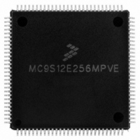
MC9S12E256MPVE Freescale Semiconductor, MC9S12E256MPVE Datasheet - Page 478

MC9S12E256MPVE
Manufacturer Part Number
MC9S12E256MPVE
Description
IC MCU 256K FLASH 25MHZ 112-LQFP
Manufacturer
Freescale Semiconductor
Series
HCS12r
Specifications of MC9S12E256MPVE
Core Processor
HCS12
Core Size
16-Bit
Speed
25MHz
Connectivity
EBI/EMI, I²C, SCI, SPI
Peripherals
POR, PWM, WDT
Number Of I /o
91
Program Memory Size
256KB (256K x 8)
Program Memory Type
FLASH
Ram Size
16K x 8
Voltage - Supply (vcc/vdd)
2.35 V ~ 2.75 V
Data Converters
A/D 16x10b; D/A 2x8b
Oscillator Type
Internal
Operating Temperature
-40°C ~ 125°C
Package / Case
112-LQFP
Processor Series
S12E
Core
HCS12
Data Bus Width
16 bit
Data Ram Size
16 KB
Interface Type
I2C/SCI/SPI
Maximum Clock Frequency
50 MHz
Number Of Programmable I/os
92
Number Of Timers
12
Operating Supply Voltage
0 V to 5 V
Maximum Operating Temperature
+ 125 C
Mounting Style
SMD/SMT
3rd Party Development Tools
EWHCS12
Minimum Operating Temperature
- 40 C
On-chip Adc
16-ch x 10-bit
On-chip Dac
2-ch x 8-bit
For Use With
M68EVB912E128 - BOARD EVAL FOR MC9S12E128/64
Lead Free Status / RoHS Status
Lead free / RoHS Compliant
Eeprom Size
-
Lead Free Status / Rohs Status
Lead free / RoHS Compliant
Available stocks
Company
Part Number
Manufacturer
Quantity
Price
Company:
Part Number:
MC9S12E256MPVE
Manufacturer:
Freescale Semiconductor
Quantity:
10 000
- Current page: 478 of 602
- Download datasheet (4Mb)
Chapter 16 Debug Module (DBGV1)
16.3.2.2
478
Reset
Field
TRG
AF
BF
CF
3:0
7
6
5
W
R
Trigger A Match Flag — The AF bit indicates if trigger A match condition was met since arming. This bit is
cleared when ARM in DBGC1 is written to a 1 or on any write to this register.
0 Trigger A did not match
1 Trigger A match
Trigger B Match Flag — The BF bit indicates if trigger B match condition was met since arming.This bit is cleared
when ARM in DBGC1 is written to a 1 or on any write to this register.
0 Trigger B did not match
1 Trigger B match
Comparator C Match Flag — The CF bit indicates if comparator C match condition was met since arming.This
bit is cleared when ARM in DBGC1 is written to a 1 or on any write to this register.
0 Comparator C did not match
1 Comparator C match
Trigger Mode Bits — The TRG bits select the trigger mode of the DBG module as shown
Section 16.4.2.5, “Trigger
AF
Debug Status and Control Register (DBGSC)
0
7
= Unimplemented or Reserved
Figure 16-5. Debug Status and Control Register (DBGSC)
BF
0
6
TRG Value
Table 16-5. DBGSC Field Descriptions
Modes,” for more detail.
Table 16-6. Trigger Mode Encoding
0000
0001
0010
0011
0100
0101
0110
0111
1000
1001
1111
MC9S12E256 Data Sheet, Rev. 1.08
CF
0
5
0
0
4
A and Not B (full mode)
Description
A then event only B
A and B (full mode)
(Defaults to A only)
Outside range
Event only B
Inside range
Reserved
Meaning
A then B
A only
A or B
3
0
0
2
TRG
Freescale Semiconductor
0
1
Table
16-6. See
0
0
Related parts for MC9S12E256MPVE
Image
Part Number
Description
Manufacturer
Datasheet
Request
R
Part Number:
Description:
Manufacturer:
Freescale Semiconductor, Inc
Datasheet:
Part Number:
Description:
Manufacturer:
Freescale Semiconductor, Inc
Datasheet:
Part Number:
Description:
Manufacturer:
Freescale Semiconductor, Inc
Datasheet:
Part Number:
Description:
Manufacturer:
Freescale Semiconductor, Inc
Datasheet:
Part Number:
Description:
Manufacturer:
Freescale Semiconductor, Inc
Datasheet:
Part Number:
Description:
Manufacturer:
Freescale Semiconductor, Inc
Datasheet:
Part Number:
Description:
Manufacturer:
Freescale Semiconductor, Inc
Datasheet:
Part Number:
Description:
Manufacturer:
Freescale Semiconductor, Inc
Datasheet:
Part Number:
Description:
Manufacturer:
Freescale Semiconductor, Inc
Datasheet:
Part Number:
Description:
Manufacturer:
Freescale Semiconductor, Inc
Datasheet:
Part Number:
Description:
Manufacturer:
Freescale Semiconductor, Inc
Datasheet:
Part Number:
Description:
Manufacturer:
Freescale Semiconductor, Inc
Datasheet:
Part Number:
Description:
Manufacturer:
Freescale Semiconductor, Inc
Datasheet:
Part Number:
Description:
Manufacturer:
Freescale Semiconductor, Inc
Datasheet:
Part Number:
Description:
Manufacturer:
Freescale Semiconductor, Inc
Datasheet:


