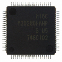
M30280FAHP#U5B Renesas Electronics America, M30280FAHP#U5B Datasheet - Page 341

M30280FAHP#U5B
Manufacturer Part Number
M30280FAHP#U5B
Description
IC M16C/28 MCU FLASH 96K 80LQFP
Manufacturer
Renesas Electronics America
Series
M16C™ M16C/Tiny/28r
Specifications of M30280FAHP#U5B
Core Size
16-Bit
Program Memory Size
96KB (96K x 8)
Core Processor
M16C/60
Speed
20MHz
Connectivity
I²C, IEBus, SIO, UART/USART
Peripherals
DMA, POR, PWM, Voltage Detect, WDT
Number Of I /o
71
Program Memory Type
FLASH
Ram Size
8K x 8
Voltage - Supply (vcc/vdd)
2.7 V ~ 5.5 V
Data Converters
A/D 24x10b
Oscillator Type
Internal
Operating Temperature
-20°C ~ 85°C
Package / Case
80-LQFP
Controller Family/series
M16C
No. Of I/o's
71
Ram Memory Size
8KB
Cpu Speed
20MHz
No. Of Timers
10
Digital Ic Case Style
LQFP
Embedded Interface Type
I2C, UART
Rohs Compliant
Yes
Lead Free Status / RoHS Status
Lead free / RoHS Compliant
For Use With
R0K330290S000BE - KIT EVAL STARTER FOR M16C/29M30290T2-CPE - EMULATOR COMPACT M16C/26A/28/29M30290T2-CPE-HP - EMULATOR COMPACT FOR M16C/TINY
Eeprom Size
-
Lead Free Status / RoHS Status
Lead free / RoHS Compliant, Lead free / RoHS Compliant
Available stocks
Company
Part Number
Manufacturer
Quantity
Price
- Current page: 341 of 425
- Download datasheet (4Mb)
M
R
R
1
e
E
Table 18.7 Errors and FMR0 Register Status
NOTE:
. v
6
J
18.8.4 Full Status Check
FMR07
0
C
(SR5)
2
9
If an error occurs, the FMR06 to FMR07 bits in the FMR0 register are set to “1”, indicating a specific error.
Therefore, execution results can be comfirmed by verifying these status bits (full status check).
Table 18.7 lists errors and FMR0 register state. Figure 18.15 shows a flow chart of the full status check
and handling procedure for each error.
1. The flash memory enters read array mode by writing command code ‘xxFF
2 /
0 .
B
(SRD register)
FMR0 Register
1
1
0
0
8
0
of these commands. The command code written in the first bus cycle becomes invalid.
0
G
4
J
7
a
o r
status
0 -
. n
u
2
3
p
0
FMR06
, 1
0
(SR4)
(
M
2
1
0
1
0
1
0
6
7
C
2 /
page 319
, 8
Command
sequence error • A value other than ‘xxD0
Erase error
Program error
M
1
Error
6
C
2 /
f o
8
3
) B
8
5
• An incorrect commands is written
• When the block erase command is executed on an protected block
• When the program command is executed on protected blocks
• The block erase command is executed on an unprotected block
• The program command is executed on an unprotected block but
bus cycle of the block erase command
but the program operation is not successfully completed
the program operation is not successfully completed
Error occurrence condition
16
’ or ‘xxFF
16
16
(1)
’ is written in the second
’ in the second bus cycle
18. Flash Memory Version
Related parts for M30280FAHP#U5B
Image
Part Number
Description
Manufacturer
Datasheet
Request
R

Part Number:
Description:
KIT STARTER FOR M16C/29
Manufacturer:
Renesas Electronics America
Datasheet:

Part Number:
Description:
KIT STARTER FOR R8C/2D
Manufacturer:
Renesas Electronics America
Datasheet:

Part Number:
Description:
R0K33062P STARTER KIT
Manufacturer:
Renesas Electronics America
Datasheet:

Part Number:
Description:
KIT STARTER FOR R8C/23 E8A
Manufacturer:
Renesas Electronics America
Datasheet:

Part Number:
Description:
KIT STARTER FOR R8C/25
Manufacturer:
Renesas Electronics America
Datasheet:

Part Number:
Description:
KIT STARTER H8S2456 SHARPE DSPLY
Manufacturer:
Renesas Electronics America
Datasheet:

Part Number:
Description:
KIT STARTER FOR R8C38C
Manufacturer:
Renesas Electronics America
Datasheet:

Part Number:
Description:
KIT STARTER FOR R8C35C
Manufacturer:
Renesas Electronics America
Datasheet:

Part Number:
Description:
KIT STARTER FOR R8CL3AC+LCD APPS
Manufacturer:
Renesas Electronics America
Datasheet:

Part Number:
Description:
KIT STARTER FOR RX610
Manufacturer:
Renesas Electronics America
Datasheet:

Part Number:
Description:
KIT STARTER FOR R32C/118
Manufacturer:
Renesas Electronics America
Datasheet:

Part Number:
Description:
KIT DEV RSK-R8C/26-29
Manufacturer:
Renesas Electronics America
Datasheet:

Part Number:
Description:
KIT STARTER FOR SH7124
Manufacturer:
Renesas Electronics America
Datasheet:

Part Number:
Description:
KIT STARTER FOR H8SX/1622
Manufacturer:
Renesas Electronics America
Datasheet:

Part Number:
Description:
KIT DEV FOR SH7203
Manufacturer:
Renesas Electronics America
Datasheet:


