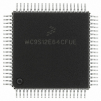
MC9S12E64CFUE Freescale Semiconductor, MC9S12E64CFUE Datasheet - Page 478

MC9S12E64CFUE
Manufacturer Part Number
MC9S12E64CFUE
Description
IC MCU 64K FLASH 25MHZ 80-QFP
Manufacturer
Freescale Semiconductor
Series
HCS12r
Specifications of MC9S12E64CFUE
Core Processor
HCS12
Core Size
16-Bit
Speed
25MHz
Connectivity
EBI/EMI, I²C, SCI, SPI
Peripherals
POR, PWM, WDT
Number Of I /o
60
Program Memory Size
64KB (64K x 8)
Program Memory Type
FLASH
Ram Size
4K x 8
Voltage - Supply (vcc/vdd)
2.35 V ~ 2.75 V
Data Converters
A/D 16x10b; D/A 2x8b
Oscillator Type
Internal
Operating Temperature
-40°C ~ 85°C
Package / Case
80-QFP
Package
80PQFP
Family Name
HCS12
Maximum Speed
25 MHz
Operating Supply Voltage
2.5|3.3|5 V
Data Bus Width
16 Bit
Number Of Programmable I/os
60
Interface Type
SCI/SPI
On-chip Adc
16-chx10-bit
On-chip Dac
2-chx8-bit
Number Of Timers
12
Processor Series
S12E
Core
HCS12
Data Ram Size
4 KB
Maximum Clock Frequency
25 MHz
Maximum Operating Temperature
+ 85 C
Mounting Style
SMD/SMT
3rd Party Development Tools
EWHCS12
Minimum Operating Temperature
- 40 C
Controller Family/series
HCS12/S12X
No. Of I/o's
58
Ram Memory Size
4KB
Cpu Speed
25MHz
No. Of Timers
4
Embedded Interface Type
I2C, SCI, SPI
Rohs Compliant
Yes
For Use With
M68EVB912E128 - BOARD EVAL FOR MC9S12E128/64
Lead Free Status / RoHS Status
Lead free / RoHS Compliant
Eeprom Size
-
Lead Free Status / Rohs Status
Lead free / RoHS Compliant
Available stocks
Company
Part Number
Manufacturer
Quantity
Price
Company:
Part Number:
MC9S12E64CFUE
Manufacturer:
Freescale Semiconductor
Quantity:
10 000
Part Number:
MC9S12E64CFUE
Manufacturer:
FREESCALE
Quantity:
20 000
Company:
Part Number:
MC9S12E64CFUER
Manufacturer:
Freescale Semiconductor
Quantity:
10 000
- Current page: 478 of 606
- Download datasheet (4Mb)
Chapter 16 Debug Module (DBGV1)
16.3
A summary of the registers associated with the DBG sub-block is shown in
descriptions of the registers and bits are given in the subsections that follow.
16.3.1
16.3.2
This section consists of the DBG register descriptions in address order. Most of the register bits can be
written to in either BKP or DBG mode, although they may not have any effect in one of the modes.
However, the only bits in the DBG module that can be written while the debugger is armed (ARM = 1) are
DBGEN and ARM
478
DBGSC
DBGC1
Name
Memory Map and Register Definition
Address
1
Offset
Module Memory Map
Register Descriptions
A
B
E
F
4
5
6
8
9
W
W
R
R
Debug Control Register (DBGC1)
Debug Status and Control Register (DBGSC)
Debug Trace Buffer Register High (DBGTBH)
Debug Trace Buffer Register Low (DBGTBL)
Debug Control Register 2 (DBGC2) / (BKPCT0)
Debug Control Register 3 (DBGC3) / (BKPCT1)
Debug Comparator A Extended Register (DBGCAX) / (/BKP0X)
Debug Comparator A Register High (DBGCAH) / (BKP0H)
Debug Comparator A Register Low (DBGCAL) / (BKP0L)
Debug Comparator B Extended Register (DBGCBX) / (BKP1X)
Debug Comparator B Register High (DBGCBH) / (BKP1H)
Debug Comparator B Register Low (DBGCBL) / (BKP1L)
Debug Count Register (DBGCNT)
Debug Comparator C Extended Register (DBGCCX)
Debug Comparator C Register High (DBGCCH)
Debug Comparator C Register Low (DBGCCL)
DBGEN
Bit 7
AF
= Unimplemented or Reserved
Figure 16-3. DBG Register Summary
ARM
BF
Table 16-2. DBGV1 Memory Map
6
MC9S12E128 Data Sheet, Rev. 1.07
TRGSEL
CF
5
Use
BEGIN
4
0
DBGBRK
3
Figure
2
0
TRG
16-3. Detailed
Freescale Semiconductor
Access
1
R/W
R/W
R/W
R/W
R/W
R/W
R/W
R/W
R/W
R/W
R/W
R/W
R/W
CAPMOD
R
R
R
Bit 0
Related parts for MC9S12E64CFUE
Image
Part Number
Description
Manufacturer
Datasheet
Request
R
Part Number:
Description:
Manufacturer:
Freescale Semiconductor, Inc
Datasheet:
Part Number:
Description:
Manufacturer:
Freescale Semiconductor, Inc
Datasheet:
Part Number:
Description:
Manufacturer:
Freescale Semiconductor, Inc
Datasheet:
Part Number:
Description:
Manufacturer:
Freescale Semiconductor, Inc
Datasheet:
Part Number:
Description:
Manufacturer:
Freescale Semiconductor, Inc
Datasheet:
Part Number:
Description:
Manufacturer:
Freescale Semiconductor, Inc
Datasheet:
Part Number:
Description:
Manufacturer:
Freescale Semiconductor, Inc
Datasheet:
Part Number:
Description:
Manufacturer:
Freescale Semiconductor, Inc
Datasheet:
Part Number:
Description:
Manufacturer:
Freescale Semiconductor, Inc
Datasheet:
Part Number:
Description:
Manufacturer:
Freescale Semiconductor, Inc
Datasheet:
Part Number:
Description:
Manufacturer:
Freescale Semiconductor, Inc
Datasheet:
Part Number:
Description:
Manufacturer:
Freescale Semiconductor, Inc
Datasheet:
Part Number:
Description:
Manufacturer:
Freescale Semiconductor, Inc
Datasheet:
Part Number:
Description:
Manufacturer:
Freescale Semiconductor, Inc
Datasheet:
Part Number:
Description:
Manufacturer:
Freescale Semiconductor, Inc
Datasheet:


