MC9S12E64CFUE Freescale Semiconductor, MC9S12E64CFUE Datasheet - Page 442
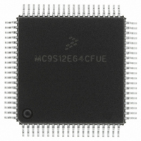
MC9S12E64CFUE
Manufacturer Part Number
MC9S12E64CFUE
Description
IC MCU 64K FLASH 25MHZ 80-QFP
Manufacturer
Freescale Semiconductor
Series
HCS12r
Specifications of MC9S12E64CFUE
Core Processor
HCS12
Core Size
16-Bit
Speed
25MHz
Connectivity
EBI/EMI, I²C, SCI, SPI
Peripherals
POR, PWM, WDT
Number Of I /o
60
Program Memory Size
64KB (64K x 8)
Program Memory Type
FLASH
Ram Size
4K x 8
Voltage - Supply (vcc/vdd)
2.35 V ~ 2.75 V
Data Converters
A/D 16x10b; D/A 2x8b
Oscillator Type
Internal
Operating Temperature
-40°C ~ 85°C
Package / Case
80-QFP
Package
80PQFP
Family Name
HCS12
Maximum Speed
25 MHz
Operating Supply Voltage
2.5|3.3|5 V
Data Bus Width
16 Bit
Number Of Programmable I/os
60
Interface Type
SCI/SPI
On-chip Adc
16-chx10-bit
On-chip Dac
2-chx8-bit
Number Of Timers
12
Processor Series
S12E
Core
HCS12
Data Ram Size
4 KB
Maximum Clock Frequency
25 MHz
Maximum Operating Temperature
+ 85 C
Mounting Style
SMD/SMT
3rd Party Development Tools
EWHCS12
Minimum Operating Temperature
- 40 C
Controller Family/series
HCS12/S12X
No. Of I/o's
58
Ram Memory Size
4KB
Cpu Speed
25MHz
No. Of Timers
4
Embedded Interface Type
I2C, SCI, SPI
Rohs Compliant
Yes
For Use With
M68EVB912E128 - BOARD EVAL FOR MC9S12E128/64
Lead Free Status / RoHS Status
Lead free / RoHS Compliant
Eeprom Size
-
Lead Free Status / Rohs Status
Lead free / RoHS Compliant
Available stocks
Company
Part Number
Manufacturer
Quantity
Price
Company:

Part Number:
MC9S12E64CFUE
Manufacturer:
Freescale Semiconductor
Quantity:
10 000
Part Number:
MC9S12E64CFUE
Manufacturer:
FREESCALE
Quantity:
20 000
Company:
Part Number:
MC9S12E64CFUER
Manufacturer:
Freescale Semiconductor
Quantity:
10 000


Chapter 14 Dual Output Voltage Regulator (VREG3V3V2)
14.2.3
Signals V
logic. These signals are connected to device pins to allow external decoupling capacitors (100 nF...220 nF,
X7R ceramic).
In shutdown mode an external supply at V
14.2.4
Signals V
PLL and oscillator. These signals are connected to device pins to allow external decoupling capacitors
(100 nF...220 nF, X7R ceramic).
In shutdown mode an external supply at V
14.2.5
This optional signal is used to shutdown VREG3V3V2. In that case V
be provided externally. shutdown mode is entered with V
VREG3V3V2 is either in full-performance mode or in reduced-power mode.
For the connectivity of V
14.3
This subsection provides a detailed description of all registers accessible in VREG3V3V2.
14.3.1
Figure 14-2
442
DDPLL
DD
Memory Map and Register Definition
Address
0x0000
Offset
V
V
V
Module Memory Map
provides an overview of all used registers.
/V
DD
DDPLL
REGEN
Switching from FPM or RPM to shutdown of VREG3V3V2 and vice versa
is not supported while the MCU is powered.
SS
/V
, V
are the primary outputs of VREG3V3V2 that provide the power supply for the core
SSPLL
SS
, V
— Optional Regulator Enable
— Regulator Output1 (Core Logic)
are the secondary outputs of VREG3V3V2 that provide the power supply for the
SSPLL
REGEN
see device overview chapter.
— Regulator Output2 (PLL)
VREG3V3V2 Control Register (VREGCTRL)
Table 14-2. VREG3V3V2 Memory Map
MC9S12E128 Data Sheet, Rev. 1.07
DD
DDPLL
/V
SS
/V
NOTE
can replace the voltage regulator.
Use
SSPLL
REGEN
can replace the voltage regulator.
being low. If V
DD
/V
SS
and V
REGEN
Freescale Semiconductor
DDPLL
is high, the
Access
R/W
/V
SSPLL
must
Related parts for MC9S12E64CFUE
Image
Part Number
Description
Manufacturer
Datasheet
Request
R

Part Number:
Description:
Manufacturer:
Freescale Semiconductor, Inc
Datasheet:
Part Number:
Description:
Manufacturer:
Freescale Semiconductor, Inc
Datasheet:
Part Number:
Description:
Manufacturer:
Freescale Semiconductor, Inc
Datasheet:
Part Number:
Description:
Manufacturer:
Freescale Semiconductor, Inc
Datasheet:
Part Number:
Description:
Manufacturer:
Freescale Semiconductor, Inc
Datasheet:
Part Number:
Description:
Manufacturer:
Freescale Semiconductor, Inc
Datasheet:
Part Number:
Description:
Manufacturer:
Freescale Semiconductor, Inc
Datasheet:
Part Number:
Description:
Manufacturer:
Freescale Semiconductor, Inc
Datasheet:
Part Number:
Description:
Manufacturer:
Freescale Semiconductor, Inc
Datasheet:
Part Number:
Description:
Manufacturer:
Freescale Semiconductor, Inc
Datasheet:
Part Number:
Description:
Manufacturer:
Freescale Semiconductor, Inc
Datasheet:
Part Number:
Description:
Manufacturer:
Freescale Semiconductor, Inc
Datasheet:
Part Number:
Description:
Manufacturer:
Freescale Semiconductor, Inc
Datasheet:
Part Number:
Description:
Manufacturer:
Freescale Semiconductor, Inc
Datasheet:
Part Number:
Description:
Manufacturer:
Freescale Semiconductor, Inc
Datasheet: