M37542F8FP#U0 Renesas Electronics America, M37542F8FP#U0 Datasheet - Page 76

M37542F8FP#U0
Manufacturer Part Number
M37542F8FP#U0
Description
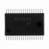
IC 740 MCU FLASH 32K 36SSOP
Manufacturer
Renesas Electronics America
Series
740/38000r
Datasheet
1.M37542F8FPU0.pdf
(124 pages)
Specifications of M37542F8FP#U0
Core Processor
740
Core Size
8-Bit
Speed
8MHz
Connectivity
SIO, UART/USART
Peripherals
WDT
Number Of I /o
29
Program Memory Size
32KB (32K x 8)
Program Memory Type
FLASH
Ram Size
1K x 8
Voltage - Supply (vcc/vdd)
2.2 V ~ 5.5 V
Data Converters
A/D 8x10b
Oscillator Type
Internal
Operating Temperature
-20°C ~ 85°C
Package / Case
36-SSOP
Lead Free Status / RoHS Status
Lead free / RoHS Compliant
Eeprom Size
-
Available stocks
Company
Part Number
Manufacturer
Quantity
Price
7542 Group
Fig. 97 Block diagram of built-in flash memory
The control program for CPU rewrite mode must be written into
the User ROM or Boot ROM area in parallel I/O mode beforehand.
(If the control program is written into the Boot ROM area, the stan-
dard serial I/O mode becomes unusable.)
See Figure 97 for details about the Boot ROM area.
Normal microcomputer mode is entered when the microcomputer
is reset with pulling CNV
operating using the control program in the User ROM area.
When the microcomputer is reset and the CNV
pulling the P3
and P0
program is stored into addresses FFFC
control program in the Boot ROM area. This mode is called the
“Boot mode”. Also, User ROM area can be rewritten using the con-
trol program in the Boot ROM area.
Block addresses refer to the maximum address of each block.
These addresses are used in the block erase command.
Rev.3.03
REJ03B0006-0303
RAM
Boot Mode
Block Address
8000
0FE0
0FFF
7000
FFFF
5
0000
0040
043F
/TxD
16
16
32K bytes ROM Product
16
16
16
16
16
16
Notes 1: The boot ROM area can be rewritten in a parallel I/O mode. (Access to except boot ROM area is disablrd.)
Internal RAM area
Internal flash memory
Internal flash memory
area
2
area
Jul 11, 2008
7
pin high, the CPU starts operating (start address of
(RP) pin low, P3
(1K bytes)
(32K bytes) (Note 3)
SFR area
SFR area
(4K bytes) (Note 3)
2: To specify a block, use the maximum address in the block.
3: The mask ROM version has the reserved ROM area. Note the difference of the area.
SS
pin low. In this case, the CPU starts
Page 74 of 117
2
(CE) pin high, P0
C000
E000
FFFF
7000
7800
8000
16
16
16
16
16
16
block 2 : 16K bytes
16
block 1 : 8K bytes
block 0 : 8K bytes
User ROM area
Data block B :
Data block A :
and FFFD
2K bytes
2K bytes
SS
6
pin high after
/S
16
CLK
) using the
RAM
pin low
0FE0
C000
0FFF
7000
7FFF
FFFF
0000
0040
043F
16
16
16K bytes ROM Product
16
16
16
16
16
16
16
Internal RAM area
Internal flash memory
Internal flash memory
area
area
(1K bytes)
(16K bytes) (Note 3)
SFR area
SFR area
(4K bytes) (Note 3)
In CPU rewrite mode, the internal flash memory can be operated
on (read, program, or erase) under control of the Central Process-
ing Unit (CPU).
In CPU rewrite mode, only the User ROM area shown in Figure 97
can be rewritten; the Boot ROM area cannot be rewritten. Make
sure the program and block erase commands are issued for only
the User ROM area and each block area.
The control program for CPU rewrite mode can be stored in either
User ROM or Boot ROM area. In the CPU rewrite mode, because
the flash memory cannot be read from the CPU, the rewrite con-
trol program must be transferred to internal RAM area before it
can be executed.
• Outline Performance
CPU rewrite mode is usable in the single-chip or Boot mode. The
only User ROM area can be rewritten.
In CPU rewrite mode, the CPU erases, programs and reads the in-
ternal flash memory as instructed by software commands. This
rewrite control program must be transferred to internal RAM area
before it can be executed.
The MCU enters CPU rewrite mode by setting “1” to the CPU re-
write mode select bit (bit 1 of address 0FE0
commands can be accepted.
Use software commands to control program and erase operations.
Whether a program or erase operation has terminated normally or
in error can be verified by reading the status register.
CPU Rewrite Mode
C000
E000
FFFF
7000
7800
7FFF
16
16
16
16
16
16
block 1 : 8K bytes
block 0 : 8K bytes
Data block B :
Data block A :
SFR area
2K bytes
2K bytes
FFFF
F000
16
16
16
). Then, software
Boot ROM area
4K bytes


