M37542F8FP#U0 Renesas Electronics America, M37542F8FP#U0 Datasheet - Page 118
M37542F8FP#U0
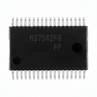
Manufacturer Part Number
M37542F8FP#U0
Description
IC 740 MCU FLASH 32K 36SSOP
Manufacturer
Renesas Electronics America
Series
740/38000r
Datasheet
1.M37542F8FPU0.pdf
(124 pages)
Specifications of M37542F8FP#U0
Core Processor
740
Core Size
8-Bit
Speed
8MHz
Connectivity
SIO, UART/USART
Peripherals
WDT
Number Of I /o
29
Program Memory Size
32KB (32K x 8)
Program Memory Type
FLASH
Ram Size
1K x 8
Voltage - Supply (vcc/vdd)
2.2 V ~ 5.5 V
Data Converters
A/D 8x10b
Oscillator Type
Internal
Operating Temperature
-20°C ~ 85°C
Package / Case
36-SSOP
Lead Free Status / RoHS Status
Lead free / RoHS Compliant
Eeprom Size
-
Available stocks
Company
Part Number
Manufacturer
Quantity
Price


7542 Group
Notes on Clock Generating Circuit
1. Switch of ceramic and RC oscillations
After releasing reset, the oscillation mode selection bit (bit 5 of
CPU mode register (address 3B
lected). When the RC oscillation is used, after releasing reset, set
this bit to “1”.
2. Double-speed mode
The double-speed mode can be used only when a ceramic oscilla-
tion is selected. Do not use it when an RC oscillation is selected.
3. CPU mode register
Oscillation mode selection bit (bit 5), processor mode bits (bits 1
and 0) of CPU mode register (address 3B
cillation mode and to control operation modes of the
microcomputer. In order to prevent the dead-lock by erroneously
writing (ex. program run-away), these bits can be rewritten only
once after releasing reset. After rewriting, it is disabled to write any
data to the bit. (The emulator MCU “M37542RSS” is excluded.)
Also, when the read-modify-write instructions (SEB, CLB, etc.) are
executed to bits 2 to 4, 6 and 7, bits 5, 1 and 0 are locked.
4. Clock division ratio, X
control
The state transition shown in Fig. 84 can be performed by setting
the clock division ratio selection bits (bits 7 and 6), X
control bit (bit 4), on-chip oscillator oscillation control bit (bit 3) of
CPU mode register. Be careful of notes on use in Fig. 84.
5. On-chip oscillator operation
When the MCU operates by the on-chip oscillator for the main
clock, connect X
leave X
The clock frequency of the on-chip oscillator depends on the sup-
ply voltage and the operation temperature range.
Be careful that this margin of frequencies when designing applica-
tion products.
6. Ceramic resonator
When the ceramic resonator is used for the main clock, connect
the ceramic resonator and the external circuit to pins X
X
tor Rd depending on the oscillation frequency. A feedback resistor
is built-in.
Use the resonator manufacturer’s recommended value because
constants such as capacitance depend on the resonator.
7. RC oscillation
When the RC oscillation is used for the main clock, connect the
X
capacitor C at the shortest distance.
The frequency is affected by a capacitor, a resistor and a micro-
computer.
So, set the constants within the range of the frequency limits.
Rev.3.03
REJ03B0006-0303
OUT
IN
pin and X
at the shortest distance. Externally connect a damping resis-
OUT
pin open.
OUT
Jul 11, 2008
IN
pin to the external circuit of resistor R and the
pin to V
IN
CC
oscillation control, on-chip oscillator
through a 1 kΩ to 10 kΩ resistor and
Page 116 of 117
16
)) is “0” (ceramic oscillation se-
16
) are used to select os-
IN
oscillation
IN
and
8. External clock
When the external signal clock is used for the main clock, connect
the X
Select “0” (ceramic oscillation) to oscillation mode selection bit.
9. Count source (Timer 1, Timer A, Timer B, Timer X, Serial I/O,
Notes on Oscillation Control
1. Oscillation stop detection circuit
(1) When the stop mode is used, set the oscillation stop detection
(2) When the ceramic or RC oscillation is stopped by the X
2. Stop mode
(1) When the stop mode is used, set the oscillation stop detection
(2) When the stop mode is used, set “0” (STP instruction enabled)
(3) The oscillation stabilizing time after release of STP instruction
(4) Do not execute the STP instruction during the A/D conversion.
Serial I/O2, A/D converter, Watchdog timer)
A count source of watchdog timer is affected by the clock divi-
sion selection bit of the CPU mode register.
The f(X
ing f(X
The on-chip oscillator output is supplied to the watchdog timer
when selecting the on-chip oscillator output as the CPU clock.
function to “invalid”.
lation control bit (bit 4 of CPU mode register (address 3B
set the oscillation stop detection function to “invalid”.
function to “invalid”.
to the STP instruction function selection bit of the watchdog
timer control register (bit 6 of watchdog timer control register
(address 39
can be selected from “set automatically ”/“not set automati-
cally” by the oscillation stabilizing time set bit after release of
the STP instruction (bit 0 of MISRG (address 38
is set to this bit, “01
prescaler 1 automatically at the execution of the STP instruc-
tion. When “1” is set to this bit, set the wait time to timer 1 and
prescaler 1 according to the oscillation stabilizing time of the
oscillation. Also, when timer 1 is used, set values again to
timer 1 and prescaler 1 after system is returned from the stop
mode.
IN
pin to the clock source and leave X
IN
IN
) as the CPU clock.
) clock is supplied to the watchdog timer when select-
16
)).
16
” is set to timer 1 and “FF
OUT
pin open.
16
)). When “0”
16
” is set to
IN
oscil-
16
)),
Related parts for M37542F8FP#U0
Image
Part Number
Description
Manufacturer
Datasheet
Request
R

Part Number:
Description:
KIT STARTER FOR M16C/29
Manufacturer:
Renesas Electronics America
Datasheet:

Part Number:
Description:
KIT STARTER FOR R8C/2D
Manufacturer:
Renesas Electronics America
Datasheet:

Part Number:
Description:
R0K33062P STARTER KIT
Manufacturer:
Renesas Electronics America
Datasheet:

Part Number:
Description:
KIT STARTER FOR R8C/23 E8A
Manufacturer:
Renesas Electronics America
Datasheet:

Part Number:
Description:
KIT STARTER FOR R8C/25
Manufacturer:
Renesas Electronics America
Datasheet:

Part Number:
Description:
KIT STARTER H8S2456 SHARPE DSPLY
Manufacturer:
Renesas Electronics America
Datasheet:

Part Number:
Description:
KIT STARTER FOR R8C38C
Manufacturer:
Renesas Electronics America
Datasheet:

Part Number:
Description:
KIT STARTER FOR R8C35C
Manufacturer:
Renesas Electronics America
Datasheet:

Part Number:
Description:
KIT STARTER FOR R8CL3AC+LCD APPS
Manufacturer:
Renesas Electronics America
Datasheet:
Part Number:
Description:
KIT STARTER FOR RX610
Manufacturer:
Renesas Electronics America
Datasheet:

Part Number:
Description:
KIT STARTER FOR R32C/118
Manufacturer:
Renesas Electronics America
Datasheet:

Part Number:
Description:
KIT DEV RSK-R8C/26-29
Manufacturer:
Renesas Electronics America
Datasheet:

Part Number:
Description:
KIT STARTER FOR SH7124
Manufacturer:
Renesas Electronics America
Datasheet:

Part Number:
Description:
KIT STARTER FOR H8SX/1622
Manufacturer:
Renesas Electronics America
Datasheet:

Part Number:
Description:
KIT DEV FOR SH7203
Manufacturer:
Renesas Electronics America
Datasheet: