SCF5250LAG100 Freescale Semiconductor, SCF5250LAG100 Datasheet - Page 5
SCF5250LAG100
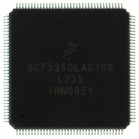
Manufacturer Part Number
SCF5250LAG100
Description
IC MPU COLDFIRE 100MHZ 144-LQFP
Manufacturer
Freescale Semiconductor
Series
SCF52xxr
Datasheet
1.SCFLXRAYADPTS12.pdf
(56 pages)
Specifications of SCF5250LAG100
Core Processor
Coldfire V2
Core Size
32-Bit
Speed
100MHz
Connectivity
EBI/EMI, I²C, IDE, MMC, SPI, UART/USART
Peripherals
DMA, I²S, POR, Serial Audio, WDT
Number Of I /o
57
Program Memory Type
ROMless
Ram Size
128K x 8
Voltage - Supply (vcc/vdd)
1.08 V ~ 1.32 V
Data Converters
A/D 6x12b
Oscillator Type
Internal
Operating Temperature
-20°C ~ 70°C
Package / Case
144-LQFP
Eeprom Size
-
Program Memory Size
-
Available stocks
Company
Part Number
Manufacturer
Quantity
Price
Company:

Part Number:
SCF5250LAG100
Manufacturer:
Intersil
Quantity:
90
Company:
Part Number:
SCF5250LAG100
Manufacturer:
Freescale Semiconductor
Quantity:
10 000
Part Number:
SCF5250LAG100
Manufacturer:
FREESCALE
Quantity:
20 000


The CD-ROM decoder performs following functions in hardware:
The CD-ROM encoder performs following functions in hardware:
1.2.13
Two full-duplex UARTs with independent receive and transmit buffers are in this module. Data formats
can be 5, 6, 7, or 8 bits with even, odd, or no parity, and up to 2 stop bits in 1/16 increments. Four-byte
receive buffers and two-byte transmit buffers minimize CPU service calls. The Dual UART module also
provides several error-detection and maskable-interrupt capabilities. Modem support includes
request-to-send (RTS) and clear-to-send (CTS) lines.
The system clock provides the clocking function from a programmable prescaler. You can select full
duplex, auto-echo loopback, local loopback, and remote loopback modes. The programmable Dual UARTs
can interrupt the CPU on various normal or error-condition events.
1.2.14
The QSPI module provides a serial peripheral interface with queued transfer capability. It supports up to
16 stacked transfers at a time, making CPU intervention between transfers unnecessary. Transfers of up to
15 Mbits/second are possible at a CPU clock of 120 MHz. The QSPI supports master mode operation only.
1.2.15
The timer module includes two general-purpose timers, each of which contains a free-running 16-bit timer.
Timer0 has an external pin TOUT0, which can be used in Output Compare mode. This mode triggers an
external signal or interrupts the CPU when the timer reaches a set value, and can also generate waveforms
on TOUT0.
The timer unit has an 8-bit prescaler that allows programming of the clock input frequency, which is
derived from the system clock. In addition to the ÷1 and ÷16 clock derived from the bus clock (CPU clock
/ 2), the programmable timer-output pins either generate an active-low pulse or toggle the outputs.
Freescale Semiconductor
•
•
•
•
•
•
•
•
Sector sync recognition
Descrambling of sectors
Verification of the CRC checksum for Mode 1, Mode 2 Form 1, and Mode 2 Form 2 sectors
Third-layer error correction is not performed
Sector sync recognition
Scrambling of sectors
Insertion of the CRC checksum for Mode 1, Mode 2 Form 1, and Mode 2 Form 2 sectors.
Third-layer error encoding needs to be done in software. This can use approximately 5–10 MHz of
performance for single-speed.
Dual UART Module
Queued Serial Peripheral Interface QSPI
Timer Module
SCF5250 Data Sheet:
Technical
Data,
Rev. 1.3
5
Related parts for SCF5250LAG100
Image
Part Number
Description
Manufacturer
Datasheet
Request
R

Part Number:
Description:
Scf5250 Integrated Coldfire Microprocessor Data Sheet
Manufacturer:
Freescale Semiconductor, Inc
Datasheet:
Part Number:
Description:
Manufacturer:
Freescale Semiconductor, Inc
Datasheet:
Part Number:
Description:
Manufacturer:
Freescale Semiconductor, Inc
Datasheet:
Part Number:
Description:
Manufacturer:
Freescale Semiconductor, Inc
Datasheet:
Part Number:
Description:
Manufacturer:
Freescale Semiconductor, Inc
Datasheet:
Part Number:
Description:
Manufacturer:
Freescale Semiconductor, Inc
Datasheet:
Part Number:
Description:
Manufacturer:
Freescale Semiconductor, Inc
Datasheet:
Part Number:
Description:
Manufacturer:
Freescale Semiconductor, Inc
Datasheet:
Part Number:
Description:
Manufacturer:
Freescale Semiconductor, Inc
Datasheet:
Part Number:
Description:
Manufacturer:
Freescale Semiconductor, Inc
Datasheet:
Part Number:
Description:
Manufacturer:
Freescale Semiconductor, Inc
Datasheet:
Part Number:
Description:
Manufacturer:
Freescale Semiconductor, Inc
Datasheet:
Part Number:
Description:
Manufacturer:
Freescale Semiconductor, Inc
Datasheet:
Part Number:
Description:
Manufacturer:
Freescale Semiconductor, Inc
Datasheet:
Part Number:
Description:
Manufacturer:
Freescale Semiconductor, Inc
Datasheet: