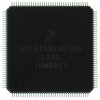
SCF5250LAG100 Freescale Semiconductor, SCF5250LAG100 Datasheet - Page 28

SCF5250LAG100
Manufacturer Part Number
SCF5250LAG100
Description
IC MPU COLDFIRE 100MHZ 144-LQFP
Manufacturer
Freescale Semiconductor
Series
SCF52xxr
Datasheet
1.SCFLXRAYADPTS12.pdf
(56 pages)
Specifications of SCF5250LAG100
Core Processor
Coldfire V2
Core Size
32-Bit
Speed
100MHz
Connectivity
EBI/EMI, I²C, IDE, MMC, SPI, UART/USART
Peripherals
DMA, I²S, POR, Serial Audio, WDT
Number Of I /o
57
Program Memory Type
ROMless
Ram Size
128K x 8
Voltage - Supply (vcc/vdd)
1.08 V ~ 1.32 V
Data Converters
A/D 6x12b
Oscillator Type
Internal
Operating Temperature
-20°C ~ 70°C
Package / Case
144-LQFP
Eeprom Size
-
Program Memory Size
-
Available stocks
Company
Part Number
Manufacturer
Quantity
Price
Company:
Part Number:
SCF5250LAG100
Manufacturer:
Intersil
Quantity:
90
Company:
Part Number:
SCF5250LAG100
Manufacturer:
Freescale Semiconductor
Quantity:
10 000
Part Number:
SCF5250LAG100
Manufacturer:
FREESCALE
Quantity:
20 000
Figure 5
28
1
2
3
4
AC timing specs assume 40pF load capacitance on BCLK and a 50pF load capacitance on output pins. If this value is different,
the input and output timing specifications would need to be adjusted to match the clock load.
Outputs (8mA): DATA[31:16], ADDR[25,23:9]
Outputs (4mA): SDRAS, SDCAS, SDWE, SD_CS0, SDUDQM, SDLDQM, BCLKE
High Impedance (Three-State): DATA[31:16]
Num
H1
H2
and
1
2
AC timing specs assume 50pF load capacitance on PSTCLK and output pins. If this value is different, the input and
output timing specifications would need to be adjusted to match the clock load.
DSCLK and DSI are internally synchronized. This setup time must be met only if recognition on a particular clock is
required.
DDATA[3:0]
Num
D3
Table 23
D1
D2
D4
PSTCLK
PST[3:0]
2
HIZ to High Impedance
HIZ to Low Impedance
DSCLK
DSO
DSI
PSTCLK to signal Valid (Output valid)
PSTCLK to signal Invalid (Output hold)
Signal Valid to PSTCLK (Input setup)
PSTCLK to signal Invalid (Input hold)
provide the timing diagram and timing parameters for the Debug AC.
Table 22. Output AC Timing Specification (continued)
Figure 5. Debug AC Timing Definition Diagram
Table 23. Debug AC Timing Specification
SCF5250 Data Sheet:
Characteristic
Characteristic
1
Technical
D3
D3
Data,
D1
Rev. 1.3
Min
1.8
–
3
5
Min
1
–
–
D4
Max
6
–
–
–
Max
tbd
tbd
Freescale Semiconductor
D4
Units
ns
ns
ns
ns
D2
Units
ns
ns


