SCF5250LAG100 Freescale Semiconductor, SCF5250LAG100 Datasheet - Page 3
SCF5250LAG100
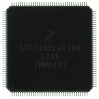
Manufacturer Part Number
SCF5250LAG100
Description
IC MPU COLDFIRE 100MHZ 144-LQFP
Manufacturer
Freescale Semiconductor
Series
SCF52xxr
Datasheet
1.SCFLXRAYADPTS12.pdf
(56 pages)
Specifications of SCF5250LAG100
Core Processor
Coldfire V2
Core Size
32-Bit
Speed
100MHz
Connectivity
EBI/EMI, I²C, IDE, MMC, SPI, UART/USART
Peripherals
DMA, I²S, POR, Serial Audio, WDT
Number Of I /o
57
Program Memory Type
ROMless
Ram Size
128K x 8
Voltage - Supply (vcc/vdd)
1.08 V ~ 1.32 V
Data Converters
A/D 6x12b
Oscillator Type
Internal
Operating Temperature
-20°C ~ 70°C
Package / Case
144-LQFP
Eeprom Size
-
Program Memory Size
-
Available stocks
Company
Part Number
Manufacturer
Quantity
Price
Company:

Part Number:
SCF5250LAG100
Manufacturer:
Intersil
Quantity:
90
Company:
Part Number:
SCF5250LAG100
Manufacturer:
Freescale Semiconductor
Quantity:
10 000
Part Number:
SCF5250LAG100
Manufacturer:
FREESCALE
Quantity:
20 000


1.2.2
The SCF5250 provides four fully programmable DMA channels for quick data transfer. Single and dual
address mode is supported with the ability to program bursting and cycle stealing. Data transfer is
selectable as 8, 16, 32, or 128-bits. Packing and unpacking is supported.
Two internal audio channels and the dual UART can be used with the DMA channels. All channels can
perform memory to memory transfers. The DMA controller has a user-selectable, 24- or 16-bit counter and
a programmable DMA exception handler.
External requests are not supported.
1.2.3
The integrated EMAC unit provides a common set of DSP operations and enhances the integer multiply
instructions in the ColdFire architecture. The EMAC provides functionality in three related areas:
Multiplies of 16x16 and 32x32 with 48-bit accumulates are supported in addition to a full set of extensions
for signed and unsigned integers plus signed, fixed-point fractional input operands. The EMAC has a
single-clock issue for 32x32-bit multiplication instructions and implements a four-stage execution
pipeline.
1.2.4
The instruction cache improves system performance by providing cached instructions to the execution unit
in a single clock. The SCF5250 processor uses a 8K-byte, direct-mapped instruction cache to achieve 107
MIPS at 120 MHz. The cache is accessed by physical addresses, where each 16-byte line consists of an
address tag and a valid bit. The instruction cache also includes a bursting interface for 16-bit and 8-bit port
sizes to quickly fill cache lines.
1.2.5
The 128-KByte on-chip SRAM is available in two banks, SRAM0 (64K) and SRAM1 (64K). It provides
one clock-cycle access for the ColdFire core. This SRAM can store processor stack and critical code or
data segments to maximize performance. Memory in SRAM1 can be accessed under DMA.
1.2.6
The SCF5250 SDRAM controller provides a glueless interface for one bank of SDRAM up to 32 MB
(256 Mbits). The controller supports a 16-bit data bus. A unique addressing scheme allows for increases
in system memory size without rerouting address lines and rewiring boards. The controller operates in
page mode, non-page mode, and burst-page mode and supports SDRAMS.
Freescale Semiconductor
1. Faster signed and unsigned integer multiplies
2. New multiply-accumulate operations supporting signed and unsigned operands
3. New miscellaneous register operations
DMA Controller
Enhanced Multiply and Accumulate Module (EMAC)
Instruction Cache
Internal 128-KByte SRAM
SDRAM Controller
SCF5250 Data Sheet:
Technical
Data,
Rev. 1.3
3
Related parts for SCF5250LAG100
Image
Part Number
Description
Manufacturer
Datasheet
Request
R

Part Number:
Description:
Scf5250 Integrated Coldfire Microprocessor Data Sheet
Manufacturer:
Freescale Semiconductor, Inc
Datasheet:
Part Number:
Description:
Manufacturer:
Freescale Semiconductor, Inc
Datasheet:
Part Number:
Description:
Manufacturer:
Freescale Semiconductor, Inc
Datasheet:
Part Number:
Description:
Manufacturer:
Freescale Semiconductor, Inc
Datasheet:
Part Number:
Description:
Manufacturer:
Freescale Semiconductor, Inc
Datasheet:
Part Number:
Description:
Manufacturer:
Freescale Semiconductor, Inc
Datasheet:
Part Number:
Description:
Manufacturer:
Freescale Semiconductor, Inc
Datasheet:
Part Number:
Description:
Manufacturer:
Freescale Semiconductor, Inc
Datasheet:
Part Number:
Description:
Manufacturer:
Freescale Semiconductor, Inc
Datasheet:
Part Number:
Description:
Manufacturer:
Freescale Semiconductor, Inc
Datasheet:
Part Number:
Description:
Manufacturer:
Freescale Semiconductor, Inc
Datasheet:
Part Number:
Description:
Manufacturer:
Freescale Semiconductor, Inc
Datasheet:
Part Number:
Description:
Manufacturer:
Freescale Semiconductor, Inc
Datasheet:
Part Number:
Description:
Manufacturer:
Freescale Semiconductor, Inc
Datasheet:
Part Number:
Description:
Manufacturer:
Freescale Semiconductor, Inc
Datasheet: