MC908GR60ACFAE Freescale Semiconductor, MC908GR60ACFAE Datasheet - Page 43
MC908GR60ACFAE
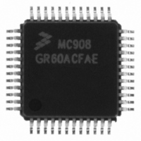
Manufacturer Part Number
MC908GR60ACFAE
Description
IC MCU 60K FLASH 8MHZ 48-LQFP
Manufacturer
Freescale Semiconductor
Series
HC08r
Datasheet
1.MC908GR32ACFJE.pdf
(314 pages)
Specifications of MC908GR60ACFAE
Core Processor
HC08
Core Size
8-Bit
Speed
8MHz
Connectivity
SCI, SPI
Peripherals
LVD, POR, PWM
Number Of I /o
37
Program Memory Size
60KB (60K x 8)
Program Memory Type
FLASH
Ram Size
2K x 8
Voltage - Supply (vcc/vdd)
3 V ~ 5.5 V
Data Converters
A/D 24x10b
Oscillator Type
Internal
Operating Temperature
-40°C ~ 85°C
Package / Case
48-LQFP
Controller Family/series
HC08
No. Of I/o's
37
Ram Memory Size
2KB
Cpu Speed
8MHz
No. Of Timers
2
Embedded Interface Type
SCI, SPI
Rohs Compliant
Yes
Processor Series
HC08GR
Core
HC08
Data Bus Width
8 bit
Data Ram Size
2 KB
Interface Type
ESCI, SPI
Maximum Clock Frequency
8 MHz
Number Of Programmable I/os
53
Number Of Timers
8
Maximum Operating Temperature
+ 85 C
Mounting Style
SMD/SMT
Development Tools By Supplier
FSICEBASE, DEMO908GZ60E, M68CBL05CE, M68EML08GPGTE
Minimum Operating Temperature
- 40 C
On-chip Adc
10 bit, 24 Channel
Lead Free Status / RoHS Status
Lead free / RoHS Compliant
Eeprom Size
-
Lead Free Status / Rohs Status
Details
Available stocks
Company
Part Number
Manufacturer
Quantity
Price
Company:

Part Number:
MC908GR60ACFAE
Manufacturer:
Freescale Semiconductor
Quantity:
10 000
Part Number:
MC908GR60ACFAE
Manufacturer:
FREESCALE
Quantity:
20 000


2.6.2.2 FLASH-1 Block Protect Register
The FLASH-1 block protect register (FL1BPR) is implemented as a byte within the FLASH-1 memory;
therefore, it can only be written during a FLASH programming sequence. The value in this register
determines the starting location of the protected range within the FLASH-1 memory.
FL1BPR[7:0] — Block Protect Register Bits 7 to 0
Freescale Semiconductor
These eight bits represent bits [14:7] of a 16-bit memory address. Bit 15 is a 1 and bits [6:0] are 0s.
The resultant 16-bit address is used for specifying the start address of the FLASH-1 memory for block
protection. FLASH-1 is protected from this start address to the end of FLASH-1 memory at $FFFF.
With this mechanism, the protect start address can be $XX00 and $XX80 (128 byte page boundaries)
within the FLASH-1 array.
Address: $FF80
Read:
Write:
MC68HC908GR60A • MC68HC908GR48A • MC68HC908GR32A Data Sheet, Rev. 5
START ADDRESS OF FLASH
Figure 2-4. FLASH-1 Block Protect Register (FL1BPR)
BPR7
Bit 7
BLOCK PROTECT
Figure 2-5. FLASH-1 Block Protect Start Address
FL1BPR[7:0]
$FF
$FE
$FD
$0B
$0A
Table 2-2. FLASH-1 Protected Ranges
$09
$08
$04
$03
$02
$01
$00
BPR6
↓
↓
6
1
BPR5
5
FLBPR VALUE
16-BIT MEMORY ADDRESS
Unaffected by reset
BPR4
4
Protected Range
$FF00–$FFFF
$FE80–$FFFF
$8580–$FFFF
$8500–$FFFF
$8480–$FFFF
$8400–$FFFF
$8200–$FFFF
$8180–$FFFF
$8100–$FFFF
$8080–$FFFF
$8000–$FFFF
No protection
BPR3
3
↓
↓
0 0 0 0 0 0 0
BPR2
2
BPR1
1
FLASH-1 Memory (FLASH-1)
BPR0
Bit 0
43
Related parts for MC908GR60ACFAE
Image
Part Number
Description
Manufacturer
Datasheet
Request
R

Part Number:
Description:
Manufacturer:
Freescale Semiconductor, Inc
Datasheet:
Part Number:
Description:
Manufacturer:
Freescale Semiconductor, Inc
Datasheet:
Part Number:
Description:
Manufacturer:
Freescale Semiconductor, Inc
Datasheet:
Part Number:
Description:
Manufacturer:
Freescale Semiconductor, Inc
Datasheet:
Part Number:
Description:
Manufacturer:
Freescale Semiconductor, Inc
Datasheet:
Part Number:
Description:
Manufacturer:
Freescale Semiconductor, Inc
Datasheet:
Part Number:
Description:
Manufacturer:
Freescale Semiconductor, Inc
Datasheet:
Part Number:
Description:
Manufacturer:
Freescale Semiconductor, Inc
Datasheet:
Part Number:
Description:
Manufacturer:
Freescale Semiconductor, Inc
Datasheet:
Part Number:
Description:
Manufacturer:
Freescale Semiconductor, Inc
Datasheet:
Part Number:
Description:
Manufacturer:
Freescale Semiconductor, Inc
Datasheet:
Part Number:
Description:
Manufacturer:
Freescale Semiconductor, Inc
Datasheet:
Part Number:
Description:
Manufacturer:
Freescale Semiconductor, Inc
Datasheet:
Part Number:
Description:
Manufacturer:
Freescale Semiconductor, Inc
Datasheet:
Part Number:
Description:
Manufacturer:
Freescale Semiconductor, Inc
Datasheet: