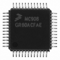
MC908GR60ACFAE Freescale Semiconductor, MC908GR60ACFAE Datasheet - Page 284

MC908GR60ACFAE
Manufacturer Part Number
MC908GR60ACFAE
Description
IC MCU 60K FLASH 8MHZ 48-LQFP
Manufacturer
Freescale Semiconductor
Series
HC08r
Datasheet
1.MC908GR32ACFJE.pdf
(314 pages)
Specifications of MC908GR60ACFAE
Core Processor
HC08
Core Size
8-Bit
Speed
8MHz
Connectivity
SCI, SPI
Peripherals
LVD, POR, PWM
Number Of I /o
37
Program Memory Size
60KB (60K x 8)
Program Memory Type
FLASH
Ram Size
2K x 8
Voltage - Supply (vcc/vdd)
3 V ~ 5.5 V
Data Converters
A/D 24x10b
Oscillator Type
Internal
Operating Temperature
-40°C ~ 85°C
Package / Case
48-LQFP
Controller Family/series
HC08
No. Of I/o's
37
Ram Memory Size
2KB
Cpu Speed
8MHz
No. Of Timers
2
Embedded Interface Type
SCI, SPI
Rohs Compliant
Yes
Processor Series
HC08GR
Core
HC08
Data Bus Width
8 bit
Data Ram Size
2 KB
Interface Type
ESCI, SPI
Maximum Clock Frequency
8 MHz
Number Of Programmable I/os
53
Number Of Timers
8
Maximum Operating Temperature
+ 85 C
Mounting Style
SMD/SMT
Development Tools By Supplier
FSICEBASE, DEMO908GZ60E, M68CBL05CE, M68EML08GPGTE
Minimum Operating Temperature
- 40 C
On-chip Adc
10 bit, 24 Channel
Lead Free Status / RoHS Status
Lead free / RoHS Compliant
Eeprom Size
-
Lead Free Status / Rohs Status
Details
Available stocks
Company
Part Number
Manufacturer
Quantity
Price
Company:
Part Number:
MC908GR60ACFAE
Manufacturer:
Freescale Semiconductor
Quantity:
10 000
Part Number:
MC908GR60ACFAE
Manufacturer:
FREESCALE
Quantity:
20 000
- Current page: 284 of 314
- Download datasheet (5Mb)
Electrical Specifications
20.9 Clock Generation Module (CGM) Characteristics
20.9.1 CGM Operating Conditions
20.9.2 CGM Component Information
284
Operating voltage
Crystal reference frequency
Input clock frequency (PLL off)
Range nominal multiplier
VCO center-of-range frequency
VCO operating frequency
Crystal frequency
Crystal load capacitance
Crystal fixed capacitance
Crystal tuning capacitance
Feedback bias resistor
Series damping resistor
V
CGMXFC filter values
1. External square wave applied to OSC1. Voltage levels must be rail-to-rail and duty cycle must be 50%.
2. Range of frequencies that VCO can produce to generate input clock to frequency divider during acquisition and tracking
3. Allowed VCO operating range.
1. Consult crystal manufacturer’s specification.
2. Capacitor on OSC1 pin. Does not include parasitic capacitance due to package, pin, and board.
3. Capacitor on OSC2 pin. Does not include parasitic capacitance due to package, pin, and board.
DDA
modes.
/V
SSA
bypass capacitor
MC68HC908GR60A • MC68HC908GR48A • MC68HC908GR32A Data Sheet, Rev. 5
Characteristic
Characteristic
(1)
(2)
(3)
(3)
(1)
(2)
Symbol
Symbol
V
f
f
f
f
V
f
C
RCLK
XCLK
f
VCLK
XCLK
NOM
VRS
C
C
C
R
R
DDA
SSA
byp
B
S
L
1
2
See
Table 4-5. Example Filter Component Values
V
V
DD
71.42k
71.42k
SS
Min
Min
—
—
—
—
—
—
—
1
1
0
– 0.3
– 0.3
(2 x C
(2 x C
71.42
Typ
Typ
0.1
20
—
—
—
—
—
—
—
1
0
L
L
) – 5
) – 5
Freescale Semiconductor
V
V
DD
SS
Max
40M
32M
Max
32
47
47
10
—
—
—
—
8
8
+ 0.3
+ 0.3
MHz
MHz
MHz
Unit
Unit
kHz
MΩ
Hz
Hz
pF
pF
pF
kΩ
μF
V
Related parts for MC908GR60ACFAE
Image
Part Number
Description
Manufacturer
Datasheet
Request
R
Part Number:
Description:
Manufacturer:
Freescale Semiconductor, Inc
Datasheet:
Part Number:
Description:
Manufacturer:
Freescale Semiconductor, Inc
Datasheet:
Part Number:
Description:
Manufacturer:
Freescale Semiconductor, Inc
Datasheet:
Part Number:
Description:
Manufacturer:
Freescale Semiconductor, Inc
Datasheet:
Part Number:
Description:
Manufacturer:
Freescale Semiconductor, Inc
Datasheet:
Part Number:
Description:
Manufacturer:
Freescale Semiconductor, Inc
Datasheet:
Part Number:
Description:
Manufacturer:
Freescale Semiconductor, Inc
Datasheet:
Part Number:
Description:
Manufacturer:
Freescale Semiconductor, Inc
Datasheet:
Part Number:
Description:
Manufacturer:
Freescale Semiconductor, Inc
Datasheet:
Part Number:
Description:
Manufacturer:
Freescale Semiconductor, Inc
Datasheet:
Part Number:
Description:
Manufacturer:
Freescale Semiconductor, Inc
Datasheet:
Part Number:
Description:
Manufacturer:
Freescale Semiconductor, Inc
Datasheet:
Part Number:
Description:
Manufacturer:
Freescale Semiconductor, Inc
Datasheet:
Part Number:
Description:
Manufacturer:
Freescale Semiconductor, Inc
Datasheet:
Part Number:
Description:
Manufacturer:
Freescale Semiconductor, Inc
Datasheet:


