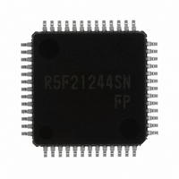
R5F21244SNFP#U0 Renesas Electronics America, R5F21244SNFP#U0 Datasheet - Page 414

R5F21244SNFP#U0
Manufacturer Part Number
R5F21244SNFP#U0
Description
IC R8C MCU FLASH 16K 52LQFP
Manufacturer
Renesas Electronics America
Series
M16C™ M16C/R8C/Tiny/24r
Datasheets
1.R5F211A2SPU0.pdf
(300 pages)
2.R5F21246SDFPU0.pdf
(61 pages)
3.R5F21246SDFPU0.pdf
(527 pages)
Specifications of R5F21244SNFP#U0
Core Processor
R8C
Core Size
16-Bit
Speed
20MHz
Connectivity
I²C, LIN, SIO, SSU, UART/USART
Peripherals
POR, Voltage Detect, WDT
Number Of I /o
41
Program Memory Size
16KB (16K x 8)
Program Memory Type
FLASH
Ram Size
1K x 8
Voltage - Supply (vcc/vdd)
2.2 V ~ 5.5 V
Data Converters
A/D 12x10b
Oscillator Type
Internal
Operating Temperature
-20°C ~ 85°C
Package / Case
52-LQFP
For Use With
R0K521256S000BE - KIT EVAL STARTER FOR R8C/25
Lead Free Status / RoHS Status
Lead free / RoHS Compliant
Eeprom Size
-
Available stocks
Company
Part Number
Manufacturer
Quantity
Price
Part Number:
R5F21244SNFP#U0R5F21244SNFP#V2
Manufacturer:
Renesas Electronics America
Quantity:
10 000
- Current page: 414 of 527
- Download datasheet (6Mb)
R8C/24 Group, R8C/25 Group
Rev.3.00
REJ09B0244-0300
18.6
Figure 18.11
To carry out A/D conversion properly, charging the internal capacitor C shown in Figure 18.11 has to be completed
within a specified period of time. T (sampling time) as the specified time. Let output impedance of sensor
equivalent circuit be R0, internal resistance of microcomputer be R, precision (error) of the A/D converter be X,
and the resolution of A/D converter be Y (Y is 1024 in the 10-bit mode, and 256 in the 8-bit mode).
Figure 18.11 shows the Analog Input Pin and External Sensor Equivalent Circuit. When the difference between
VIN and VC becomes 0.1LSB, we find impedance R0 when voltage between pins VC changes from 0 to VIN-
(0.1/1024) VIN in time T. (0.1/1024) means that A/D precision drop due to insufficient capacitor charge is held to
0.1LSB at time of A/D conversion in the 10-bit mode. Actual error however is the value of absolute precision
added to 0.1LSB.
When f(XIN) = 10 MHz, T = 0.25 µs in the A/D conversion mode without sample & hold. Output impedance R0
for sufficiently charging capacitor C within time T is determined as follows.
Thus, the allowable output impedance of the sensor equivalent circuit, making the precision (error) 0.1LSB or less,
is approximately 1.7 kΩ. maximum.
Output Impedance of Sensor under A/D Conversion
Feb 29, 2008
VC is generally
And when t = T,
Hence,
T = 0.25 µs, R = 2.8 kΩ, C = 6.0 pF, X = 0.1, and Y = 1024. Hence,
R0
Analog Input Pin and External Sensor Equivalent Circuit
=
R0
–
-------------------------------------------------- -
6.0
=
×
Page 395 of 485
–
0.25
10
VC
-------------------
C
Sensor equivalent
circuit
VC
•
–
–
e
12
T
=
×
VIN
NOTE:
ln
–
--------------------------
C R0
10
1. The capacity of the terminal is assumed to be 4.5 pF.
•
VIN 1 e
X
--- -
Y
=
--------------------------T
C R0
(
ln
(
6 –
–
VIN
1
----------- -
1024
R
0.1
1
+
+
R
–
–
R
R0
–
)
X
--- - VIN
Y
T
2.8
)
–
=
--------------------------
C R0
=
×10
ln
(
X
--- -
Y
X
--- -
Y
3
1
=
≈
+
VIN 1
1.7
R
MCU
)
×10
t
C (6.0 pF)
R (2.8 kΩ)
3
–
X
--- -
Y
VC
18. A/D Converter
Related parts for R5F21244SNFP#U0
Image
Part Number
Description
Manufacturer
Datasheet
Request
R

Part Number:
Description:
KIT STARTER FOR M16C/29
Manufacturer:
Renesas Electronics America
Datasheet:

Part Number:
Description:
KIT STARTER FOR R8C/2D
Manufacturer:
Renesas Electronics America
Datasheet:

Part Number:
Description:
R0K33062P STARTER KIT
Manufacturer:
Renesas Electronics America
Datasheet:

Part Number:
Description:
KIT STARTER FOR R8C/23 E8A
Manufacturer:
Renesas Electronics America
Datasheet:

Part Number:
Description:
KIT STARTER FOR R8C/25
Manufacturer:
Renesas Electronics America
Datasheet:

Part Number:
Description:
KIT STARTER H8S2456 SHARPE DSPLY
Manufacturer:
Renesas Electronics America
Datasheet:

Part Number:
Description:
KIT STARTER FOR R8C38C
Manufacturer:
Renesas Electronics America
Datasheet:

Part Number:
Description:
KIT STARTER FOR R8C35C
Manufacturer:
Renesas Electronics America
Datasheet:

Part Number:
Description:
KIT STARTER FOR R8CL3AC+LCD APPS
Manufacturer:
Renesas Electronics America
Datasheet:

Part Number:
Description:
KIT STARTER FOR RX610
Manufacturer:
Renesas Electronics America
Datasheet:

Part Number:
Description:
KIT STARTER FOR R32C/118
Manufacturer:
Renesas Electronics America
Datasheet:

Part Number:
Description:
KIT DEV RSK-R8C/26-29
Manufacturer:
Renesas Electronics America
Datasheet:

Part Number:
Description:
KIT STARTER FOR SH7124
Manufacturer:
Renesas Electronics America
Datasheet:

Part Number:
Description:
KIT STARTER FOR H8SX/1622
Manufacturer:
Renesas Electronics America
Datasheet:

Part Number:
Description:
KIT DEV FOR SH7203
Manufacturer:
Renesas Electronics America
Datasheet:


