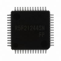
R5F21244SNFP#U0 Renesas Electronics America, R5F21244SNFP#U0 Datasheet - Page 202

R5F21244SNFP#U0
Manufacturer Part Number
R5F21244SNFP#U0
Description
IC R8C MCU FLASH 16K 52LQFP
Manufacturer
Renesas Electronics America
Series
M16C™ M16C/R8C/Tiny/24r
Datasheets
1.R5F211A2SPU0.pdf
(300 pages)
2.R5F21246SDFPU0.pdf
(61 pages)
3.R5F21246SDFPU0.pdf
(527 pages)
Specifications of R5F21244SNFP#U0
Core Processor
R8C
Core Size
16-Bit
Speed
20MHz
Connectivity
I²C, LIN, SIO, SSU, UART/USART
Peripherals
POR, Voltage Detect, WDT
Number Of I /o
41
Program Memory Size
16KB (16K x 8)
Program Memory Type
FLASH
Ram Size
1K x 8
Voltage - Supply (vcc/vdd)
2.2 V ~ 5.5 V
Data Converters
A/D 12x10b
Oscillator Type
Internal
Operating Temperature
-20°C ~ 85°C
Package / Case
52-LQFP
For Use With
R0K521256S000BE - KIT EVAL STARTER FOR R8C/25
Lead Free Status / RoHS Status
Lead free / RoHS Compliant
Eeprom Size
-
Available stocks
Company
Part Number
Manufacturer
Quantity
Price
Part Number:
R5F21244SNFP#U0R5F21244SNFP#V2
Manufacturer:
Renesas Electronics America
Quantity:
10 000
- Current page: 202 of 527
- Download datasheet (6Mb)
R8C/24 Group, R8C/25 Group
Rev.3.00
REJ09B0244-0300
Table 14.23
i = 0 or 1, j = either A, B, C, or D
Count sources
Count operations
Count period
Count start condition
Count stop condition
Interrupt request generation
timing
TRDIOA0 pin function
TRDIOB0, TRDIOC0,
TRDIOD0, TRDIOA1 to
TRDIOD1 pin functions
INT0 pin function
Read from timer
Write to timer
Select functions
Feb 29, 2008
Item
Input Capture Function Specifications
Page 183 of 485
f1, f2, f4, f8, f32, fOCO40M
External signal input to the TRDCLK pin (valid edge selected by a
program)
Increment
When bits CCLR2 to CCLR0 in the TRDCRi register are set to 000b
(free-running operation).
0 (count stops) is written to the TSTARTi bit in the TRDSTR register
when the CSELi bit in the TRDSTR register is set to 1.
• Input capture (valid edge of TRDIOji input or fOCO128 signal edge)
• TRDi register overflows
Programmable I/O port, input-capture input, or TRDCLK (external clock)
input
Programmable I/O port, or input-capture input (selectable by pin)
Programmable I/O port or INT0 interrupt input
The count value can be read by reading the TRDi register.
• When the SYNC bit in the TRDMR register is set to 0 (channels 0 and
• When the SYNC bit in the TRDMR register is set to 1 (channels 0 and
• Input-capture input pin selected
• Input-capture input valid edge selected
• The timing when the TRDi register is set to 0000h
• Buffer operation (Refer to 14.3.2 Buffer Operation.)
• Synchronous operation (Refer to 14.3.3 Synchronous Operation.)
• Digital filter
• Input-capture trigger selected
1 (count starts) is written to the TSTARTi bit in the TRDSTR register.
1 operate independently).
1 operate synchronously).
1/fk × 65536 fk: Frequency of count source
Data can be written to the TRDi register.
Data can be written to both the TRD0 and TRD1 registers by writing to
the TRDi register.
Either 1 pin or multiple pins among TRDIOAi, TRDIOBi, TRDIOCi, or
TRDIODi.
The rising edge, falling edge, or both the rising and falling edges
At overflow or input capture
The TRDIOji input is sampled, and when the sampled input level
match as 3 times, the level is determined.
fOCO128 can be selected for input-capture trigger input of the
TRDGRA0 register.
Specification
14. Timers
Related parts for R5F21244SNFP#U0
Image
Part Number
Description
Manufacturer
Datasheet
Request
R

Part Number:
Description:
KIT STARTER FOR M16C/29
Manufacturer:
Renesas Electronics America
Datasheet:

Part Number:
Description:
KIT STARTER FOR R8C/2D
Manufacturer:
Renesas Electronics America
Datasheet:

Part Number:
Description:
R0K33062P STARTER KIT
Manufacturer:
Renesas Electronics America
Datasheet:

Part Number:
Description:
KIT STARTER FOR R8C/23 E8A
Manufacturer:
Renesas Electronics America
Datasheet:

Part Number:
Description:
KIT STARTER FOR R8C/25
Manufacturer:
Renesas Electronics America
Datasheet:

Part Number:
Description:
KIT STARTER H8S2456 SHARPE DSPLY
Manufacturer:
Renesas Electronics America
Datasheet:

Part Number:
Description:
KIT STARTER FOR R8C38C
Manufacturer:
Renesas Electronics America
Datasheet:

Part Number:
Description:
KIT STARTER FOR R8C35C
Manufacturer:
Renesas Electronics America
Datasheet:

Part Number:
Description:
KIT STARTER FOR R8CL3AC+LCD APPS
Manufacturer:
Renesas Electronics America
Datasheet:

Part Number:
Description:
KIT STARTER FOR RX610
Manufacturer:
Renesas Electronics America
Datasheet:

Part Number:
Description:
KIT STARTER FOR R32C/118
Manufacturer:
Renesas Electronics America
Datasheet:

Part Number:
Description:
KIT DEV RSK-R8C/26-29
Manufacturer:
Renesas Electronics America
Datasheet:

Part Number:
Description:
KIT STARTER FOR SH7124
Manufacturer:
Renesas Electronics America
Datasheet:

Part Number:
Description:
KIT STARTER FOR H8SX/1622
Manufacturer:
Renesas Electronics America
Datasheet:

Part Number:
Description:
KIT DEV FOR SH7203
Manufacturer:
Renesas Electronics America
Datasheet:


