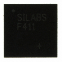
C8051F411-GM Silicon Laboratories Inc, C8051F411-GM Datasheet - Page 268

C8051F411-GM
Manufacturer Part Number
C8051F411-GM
Description
IC 8051 MCU 32K FLASH 28QFN
Manufacturer
Silicon Laboratories Inc
Series
C8051F41xr
Specifications of C8051F411-GM
Program Memory Type
FLASH
Program Memory Size
32KB (32K x 8)
Package / Case
28-QFN
Core Processor
8051
Core Size
8-Bit
Speed
50MHz
Connectivity
SMBus (2-Wire/I²C), SPI, UART/USART
Peripherals
Brown-out Detect/Reset, POR, PWM, Temp Sensor, WDT
Number Of I /o
20
Ram Size
2.25K x 8
Voltage - Supply (vcc/vdd)
2 V ~ 5.25 V
Data Converters
A/D 20x12b; D/A 2x12b
Oscillator Type
Internal
Operating Temperature
-40°C ~ 85°C
Processor Series
C8051F4x
Core
8051
Data Bus Width
8 bit
Data Ram Size
2368 B
Interface Type
I2C, SMBus, SPI, UART
Maximum Clock Frequency
50 MHz
Number Of Programmable I/os
20
Number Of Timers
4
Operating Supply Voltage
2 V to 5.25 V
Maximum Operating Temperature
+ 85 C
Mounting Style
SMD/SMT
3rd Party Development Tools
PK51, CA51, A51, ULINK2
Development Tools By Supplier
C8051F410DK
Minimum Operating Temperature
- 40 C
On-chip Adc
12 bit, 20 Channel
On-chip Dac
12 bit, 2 Channel
No. Of I/o's
20
Ram Memory Size
2368Byte
Cpu Speed
50MHz
No. Of Timers
4
Rohs Compliant
Yes
Lead Free Status / RoHS Status
Lead free / RoHS Compliant
For Use With
770-1006 - ISP 4PORT FOR SILABS C8051F MCU336-1454 - ADAPTER PROGRAM TOOLSTICK F411336-1317 - KIT EVAL FOR C8051F411336-1314 - KIT DEV FOR C8051F41X
Eeprom Size
-
Lead Free Status / Rohs Status
Lead free / RoHS Compliant
Other names
336-1309
Available stocks
Company
Part Number
Manufacturer
Quantity
Price
Company:
Part Number:
C8051F411-GM
Manufacturer:
Silicon
Quantity:
3
Part Number:
C8051F411-GM
Manufacturer:
SILICON LABS/芯科
Quantity:
20 000
Company:
Part Number:
C8051F411-GMR
Manufacturer:
SiliconL
Quantity:
3 000
Part Number:
C8051F411-GMR
Manufacturer:
SILICON LABS/芯科
Quantity:
20 000
C8051F410/1/2/3
D
Revision 0.7 to Revision 0.8
•
•
•
•
•
•
•
•
•
•
•
•
•
•
•
Revision 0.8 to Revision 1.0
•
•
•
•
•
•
Revision 1.0 to Revision 1.1
•
•
•
•
•
•
268
OCUMENT
Updated specification tables with most recently available characterization data.
Corrected references to configuring pins for Analog Mode - Port Latch must contain a '1'.
SFR Definition 5.6: Address correction to 0xBA.
Added Figure 8.2 showing power connection diagram without using on-chip regulator.
Section 9
Table 11.2 : Corrected SFR Name P2MDIN on location 0xF3.
Section 14
Section 18
last sentence.
Section 19.2.2
Section 19.3
cies.
Section 21
Table 21.4 : Made corrections to SMBus state descriptions.
Figure 24.6 : Corrected T2RCLK Mux selection options.
Figure 24.9 : Corrected T3RCLK Mux selection options.
C2 Register Definition 26.2 : Corrected DEVICEID value to 0x0C.
Updated specification tables with full characterization data.
Updated Flash write and erase procedures to include a write to FLSCL.3-0.
Changed /RST pin comments in Table 4.1, “Pin Definitions for the C8051F41x,” on page 41 for the recom-
mended pull-up resistor.
Changed the reset value of the SFR Definition 16.3. FLSCL: Flash Scale.
Removed the "Optional GND Connection" from Figure 4.5. ’Typical QFN-28 Landing Diagram’ on page 48.
Added a note regarding the maximum SYSCLK frequency to SFR Definition 19.4. CLKMUL: Clock Multi-
plier Control.
Updated Figure 4.3. ’LQFP-32 Package Diagram’ on page 46, Figure 4.5. ’QFN-28 Package Drawing’ on
page 48, and Figure 4.6. ’QFN-28 Recommended PCB Land Pattern’ on page 49.
Added note that VIO must be > VDD in Table 3.1, “Global DC Electrical Characteristics,” on page 36.
Added information about ADC0 output register auto-clearing in SFR Definition 5.2.
Corrected ADC0 Tracking time equation in SFR Definition 5.6.
Clarified Voltage Regulator Electrical Specifications in Table 8.1 on page 82.
Added information about 16-bit and 32-bit CRC algorithms in
: Removed references to "High Speed Analog Mode".
, Important Note on page 151 : Added "and have the same behavior as P0 in Normal Mode." to
: Corrected SMBus maximum rate to 1/20th system clock.
: Corrected operational description of CRC engine.
: Added Figure 19.3 and text to describe behavior of clock multiplier with slower input frequen-
C
: Inserted Step 3 "Release the crystal pins by writing ‘1's to the port latch."
HANGE
L
IST
Rev. 1.1
Section 14
.


