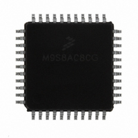
MC9S08AC8CFGE Freescale Semiconductor, MC9S08AC8CFGE Datasheet - Page 187

MC9S08AC8CFGE
Manufacturer Part Number
MC9S08AC8CFGE
Description
IC MCU 8BIT 8K FLASH 44-LQFP
Manufacturer
Freescale Semiconductor
Series
HCS08r
Datasheet
1.MC9S08AC8CFGE.pdf
(336 pages)
Specifications of MC9S08AC8CFGE
Core Processor
HCS08
Core Size
8-Bit
Speed
40MHz
Connectivity
I²C, SCI, SPI
Peripherals
LVD, POR, PWM, WDT
Number Of I /o
34
Program Memory Size
8KB (8K x 8)
Program Memory Type
FLASH
Ram Size
768 x 8
Voltage - Supply (vcc/vdd)
2.7 V ~ 5.5 V
Data Converters
A/D 8x10b
Oscillator Type
Internal
Operating Temperature
-40°C ~ 85°C
Package / Case
44-LQFP
Processor Series
S08AC
Core
HCS08
Data Bus Width
8 bit
Data Ram Size
700 B
Interface Type
I2C, SCI, SPI
Maximum Clock Frequency
40 MHz
Number Of Programmable I/os
34
Number Of Timers
3
Operating Supply Voltage
- 0.3 V to + 5.8 V
Maximum Operating Temperature
+ 125 C
Mounting Style
SMD/SMT
3rd Party Development Tools
EWS08
Development Tools By Supplier
DEMO9S08AC60E, DEMOACEX, DEMOACKIT, DCF51AC256, DC9S08AC128, DC9S08AC16, DC9S08AC60, DEMO51AC256KIT
Minimum Operating Temperature
- 40 C
On-chip Adc
10 bit, 8 Channel
Lead Free Status / RoHS Status
Lead free / RoHS Compliant
Eeprom Size
-
Lead Free Status / Rohs Status
Lead free / RoHS Compliant
Available stocks
Company
Part Number
Manufacturer
Quantity
Price
Company:
Part Number:
MC9S08AC8CFGE
Manufacturer:
Freescale Semiconductor
Quantity:
10 000
- Current page: 187 of 336
- Download datasheet (7Mb)
Freescale Semiconductor
TPMxCNTH:TPMxCNTL
TPMxMODH:TPMxMODL = 0x0007
TPMxCnVH:TPMxCnVL = 0x0005
EPWM mode
6. Write to TPMxMODH:L registers in BDM mode
7. Update of EPWM signal when CLKSB:CLKSA = 00
(in TPMv2 and TPMv3)
TPMv2 TPMxCHn
CLKSB:CLKSA BITS
TPMv3 TPMxCHn
ELSnB:ELSnA BITS
RESET (active low)
MSnB:MSnA BITS
— TPMxCnVH:L is changed from a non-zero value to 0x0000 [SE110-TPM case 4]
Registers
In the TPM v3 a write to TPMxSC register in BDM mode clears the write coherency mechanism
of TPMxMODH:L registers. Instead, in the TPM v2 this coherency mechanism is not cleared when
there is a write to TPMxSC register.
In the TPM v3 if CLKSB:CLKSA = 00, then the EPWM signal in the channel output is not update
(it is frozen while CLKSB:CLKSA = 00). Instead, in the TPM v2 the EPWM signal is updated at
the next rising edge of bus clock after a write to TPMxCnSC register.
The
v3 after the reset (CLKSB:CLKSA = 00) and if there is a write to TPMxCnSC register.
BUS CLOCK
Figure 10-17. Generation of high-true EPWM signal by TPM v2 and v3 after the reset
In this case, the TPM v3 finishes the current PWM period using the old duty cycle setting.
Instead, the TPM v2 finishes the current PWM period using the new duty cycle setting.
Figure 10-17
CHnF BIT
(TPMxMODH:TPMxMODL))
and
00
00
Figure 10-18
MC9S08AC16 Series Data Sheet, Rev. 8
show when the EPWM signals generated by TPM v2 and TPM
00
0
(Section 10.5.3, “TPM Counter Modulo
10
10
1 2 3 4 5 6 7
Timer/PWM Module (S08TPMV3)
01
0 1
2
...
187
Related parts for MC9S08AC8CFGE
Image
Part Number
Description
Manufacturer
Datasheet
Request
R
Part Number:
Description:
Manufacturer:
Freescale Semiconductor, Inc
Datasheet:
Part Number:
Description:
Manufacturer:
Freescale Semiconductor, Inc
Datasheet:
Part Number:
Description:
Manufacturer:
Freescale Semiconductor, Inc
Datasheet:
Part Number:
Description:
Manufacturer:
Freescale Semiconductor, Inc
Datasheet:
Part Number:
Description:
Manufacturer:
Freescale Semiconductor, Inc
Datasheet:
Part Number:
Description:
Manufacturer:
Freescale Semiconductor, Inc
Datasheet:
Part Number:
Description:
Manufacturer:
Freescale Semiconductor, Inc
Datasheet:
Part Number:
Description:
Manufacturer:
Freescale Semiconductor, Inc
Datasheet:
Part Number:
Description:
Manufacturer:
Freescale Semiconductor, Inc
Datasheet:
Part Number:
Description:
Manufacturer:
Freescale Semiconductor, Inc
Datasheet:
Part Number:
Description:
Manufacturer:
Freescale Semiconductor, Inc
Datasheet:
Part Number:
Description:
Manufacturer:
Freescale Semiconductor, Inc
Datasheet:
Part Number:
Description:
Manufacturer:
Freescale Semiconductor, Inc
Datasheet:
Part Number:
Description:
Manufacturer:
Freescale Semiconductor, Inc
Datasheet:
Part Number:
Description:
Manufacturer:
Freescale Semiconductor, Inc
Datasheet:


