MC68HC908JB8JPE Freescale Semiconductor, MC68HC908JB8JPE Datasheet - Page 137
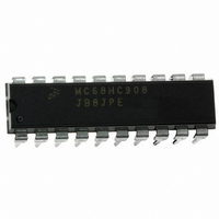
MC68HC908JB8JPE
Manufacturer Part Number
MC68HC908JB8JPE
Description
IC MCU FLASH 8BIT 8K 20-DIP
Manufacturer
Freescale Semiconductor
Series
HC08r
Datasheet
1.MC908JB8JDWE.pdf
(286 pages)
Specifications of MC68HC908JB8JPE
Core Processor
HC08
Core Size
8-Bit
Speed
3MHz
Connectivity
USB
Peripherals
LVD, POR, PWM
Number Of I /o
13
Program Memory Size
8KB (8K x 8)
Program Memory Type
FLASH
Ram Size
256 x 8
Voltage - Supply (vcc/vdd)
4 V ~ 5.5 V
Oscillator Type
Internal
Operating Temperature
0°C ~ 70°C
Package / Case
20-DIP (0.300", 7.62mm)
Controller Family/series
HC08
No. Of I/o's
13
Ram Memory Size
256Byte
Cpu Speed
3MHz
No. Of Timers
1
Embedded Interface Type
USB
Rohs Compliant
Yes
Processor Series
HC08JB
Core
HC08
Data Bus Width
8 bit
Data Ram Size
256 B
Interface Type
USB
Maximum Clock Frequency
3 MHz
Number Of Programmable I/os
37
Number Of Timers
2
Operating Supply Voltage
4 V to 5.5 V
Maximum Operating Temperature
+ 70 C
Mounting Style
Through Hole
Development Tools By Supplier
FSICEBASE, DEMO908GZ60E, M68EML08GZE, KITUSBSPIDGLEVME, KITUSBSPIEVME, KIT33810EKEVME
Minimum Operating Temperature
0 C
Lead Free Status / RoHS Status
Lead free / RoHS Compliant
Eeprom Size
-
Data Converters
-
Lead Free Status / Rohs Status
Details


9.7.3 USB Control Logic
9.8 I/O Registers
MC68HC908JB8•MC68HC08JB8•MC68HC08JT8 — Rev. 2.3
Freescale Semiconductor
The USB control logic manages data movement between the CPU and
the transceiver. The control logic handles both transmit and receive
operations on the USB. It contains the logic used to manipulate the
transceiver and the endpoint registers.
The byte count buffer is loaded with the active transmit endpoints byte
count value during transmit operations. This same buffer is used for
receive transactions to count the number of bytes received and, upon
the end of the transaction, transfer that number to the receive endpoints
byte count register.
When transmitting, the control logic handles parallel-to-serial
conversion, CRC generation, NRZI encoding, and bit stuffing.
When receiving, the control logic handles sync detection, packet
identification, end-of-packet detection, bit (un)stuffing, NRZI decoding,
CRC validation, and serial-to-parallel conversion. Errors detected by the
control logic include bad CRC, timeout while waiting for EOP, and bit
stuffing violations.
These I/O registers control and monitor USB operation:
•
•
•
•
•
•
•
USB address register (UADDR)
USB control registers 0–4 (UCR0–UCR4)
USB status registers 0–1 (USR0–USR1)
USB interrupt registers 0–2 (UIR0–UIR2)
USB endpoint 0 data registers 0–7 (UE0D0–UE0D7)
USB endpoint 1 data registers 0–7 (UE1D0–UE1D7)
USB endpoint 2 data registers 0–7 (UE2D0–UE2D7)
Universal Serial Bus Module (USB)
Universal Serial Bus Module (USB)
Technical Data
I/O Registers
137
Related parts for MC68HC908JB8JPE
Image
Part Number
Description
Manufacturer
Datasheet
Request
R

Part Number:
Description:
Manufacturer:
Freescale Semiconductor, Inc
Datasheet:
Part Number:
Description:
Manufacturer:
Freescale Semiconductor, Inc
Datasheet:
Part Number:
Description:
Manufacturer:
Freescale Semiconductor, Inc
Datasheet:
Part Number:
Description:
Manufacturer:
Freescale Semiconductor, Inc
Datasheet:
Part Number:
Description:
Manufacturer:
Freescale Semiconductor, Inc
Datasheet:
Part Number:
Description:
Manufacturer:
Freescale Semiconductor, Inc
Datasheet:
Part Number:
Description:
Manufacturer:
Freescale Semiconductor, Inc
Datasheet:
Part Number:
Description:
Manufacturer:
Freescale Semiconductor, Inc
Datasheet:
Part Number:
Description:
Manufacturer:
Freescale Semiconductor, Inc
Datasheet:
Part Number:
Description:
Manufacturer:
Freescale Semiconductor, Inc
Datasheet:
Part Number:
Description:
Manufacturer:
Freescale Semiconductor, Inc
Datasheet:
Part Number:
Description:
Manufacturer:
Freescale Semiconductor, Inc
Datasheet:
Part Number:
Description:
Manufacturer:
Freescale Semiconductor, Inc
Datasheet:
Part Number:
Description:
Manufacturer:
Freescale Semiconductor, Inc
Datasheet:
Part Number:
Description:
Manufacturer:
Freescale Semiconductor, Inc
Datasheet: