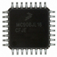
MC908JL16CFJER Freescale Semiconductor, MC908JL16CFJER Datasheet - Page 69

MC908JL16CFJER
Manufacturer Part Number
MC908JL16CFJER
Description
IC MCU 8BIT 16K FLASH 32-LQFP
Manufacturer
Freescale Semiconductor
Series
HC08r
Datasheet
1.MC908JL16CFJER.pdf
(230 pages)
Specifications of MC908JL16CFJER
Core Processor
HC08
Core Size
8-Bit
Speed
8MHz
Connectivity
I²C, SCI
Peripherals
LED, LVD, POR, PWM
Number Of I /o
26
Program Memory Size
16KB (16K x 8)
Program Memory Type
FLASH
Ram Size
512 x 8
Voltage - Supply (vcc/vdd)
2.7 V ~ 5.5 V
Data Converters
A/D 13x10b
Oscillator Type
Internal
Operating Temperature
-40°C ~ 85°C
Package / Case
32-LQFP
Controller Family/series
HC08
No. Of I/o's
26
Ram Memory Size
512Byte
Cpu Speed
8MHz
No. Of Timers
2
Digital Ic Case Style
LQFP
Rohs Compliant
Yes
Processor Series
HC08JL
Core
HC08
Data Bus Width
8 bit
Data Ram Size
512 B
Interface Type
SCI
Maximum Clock Frequency
8 MHz
Number Of Programmable I/os
26
Number Of Timers
4
Maximum Operating Temperature
+ 85 C
Mounting Style
SMD/SMT
Development Tools By Supplier
FSICEBASE, DEMO908JL16E, M68CBL05CE
Minimum Operating Temperature
- 40 C
On-chip Adc
10 bit, 13 Channel
For Use With
DEMO908JL16E - BOARD DEMO FOR MC908JL16
Lead Free Status / RoHS Status
Lead free / RoHS Compliant
Eeprom Size
-
Lead Free Status / Rohs Status
Details
Other names
MC908JL16CFJERTR
Available stocks
Company
Part Number
Manufacturer
Quantity
Price
Company:
Part Number:
MC908JL16CFJER
Manufacturer:
Freescale Semiconductor
Quantity:
29 890
Company:
Part Number:
MC908JL16CFJER
Manufacturer:
Freescale
Quantity:
198
Company:
Part Number:
MC908JL16CFJER
Manufacturer:
Freescale Semiconductor
Quantity:
10 000
Chapter 6
Timer Interface Module (TIM)
6.1 Introduction
This section describes the timer interface (TIM) module. The TIM is a two-channel timer that provides a
timing reference with Input capture, output compare, and pulse-width-modulation functions.
a block diagram of the TIM.
This particular MCU has two timer interface modules which are denoted as TIM1 and TIM2.
6.2 Features
Features of the TIM include:
6.3 Pin Name Conventions
The text that follows describes both timers, TIM1 and TIM2. The TIM input/output (I/O) pin names are
T[1,2]CH0 (timer channel 0) and T[1,2]CH1 (timer channel 1), where “1” is used to indicate TIM1 and “2”
is used to indicate TIM2. The two TIMs share four I/O pins with four I/O port pins. The external clock input
for TIM2 is shared with the an ADC channel pin. The full names of the TIM I/O pins are listed in
The generic pin names appear in the text that follows.
Freescale Semiconductor
•
•
•
•
•
•
Two input capture/output compare channels:
–
–
Buffered and unbuffered pulse-width-modulation (PWM) signal generation
Programmable TIM clock input
–
–
Free-running or modulo up-count operation
Toggle any channel pin on overflow
TIM counter stop and reset bits
Rising-edge, falling-edge, or any-edge input capture trigger
Set, clear, or toggle output compare action
7-frequency internal bus clock prescaler selection
External clock input on timer 2 (bus frequency ÷2 maximum)
References to either timer 1 or timer 2 may be made in the following text by
omitting the timer number. For example, TCH0 may refer generically to
T1CH0 and T2CH0, and TCH1 may refer to T1CH1 and T2CH1.
TIM Generic Pin Names:
Pin Names:
Full TIM
TIM1
TIM2
Table 6-1. Pin Name Conventions
MC68HC908JL16 Data Sheet, Rev. 1.1
PTD4/T1CH0
PTE0/T2CH0
T[1,2]CH0
NOTE
PTD5/T1CH1
PTE1/T2CH1
T[1,2]CH1
ADC12/T2CLK
T2CLK
—
Figure 6-1
Table
6-1.
is
69


