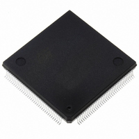
ST10F269Z2Q3 STMicroelectronics, ST10F269Z2Q3 Datasheet - Page 74

ST10F269Z2Q3
Manufacturer Part Number
ST10F269Z2Q3
Description
IC FLASH MEM 256KBIT 144-PQFP
Manufacturer
STMicroelectronics
Series
ST10r
Datasheet
1.ST10F269Z2Q3.pdf
(184 pages)
Specifications of ST10F269Z2Q3
Core Processor
ST10
Core Size
16-Bit
Speed
40MHz
Connectivity
CAN, EBI/EMI, SSC, UART/USART
Peripherals
POR, PWM, WDT
Number Of I /o
111
Program Memory Size
256KB (256K x 8)
Program Memory Type
FLASH
Ram Size
12K x 8
Voltage - Supply (vcc/vdd)
4.5 V ~ 5.5 V
Data Converters
A/D 16x10b
Oscillator Type
Internal
Operating Temperature
-40°C ~ 125°C
Package / Case
144-QFP
Processor Series
ST10F26x
Core
ST10
Data Bus Width
16 bit
Data Ram Size
12 KB
Interface Type
CAN, SSC, USART
Maximum Clock Frequency
40 MHz
Number Of Programmable I/os
111
Number Of Timers
2 x 16 bit
Operating Supply Voltage
0.3 V to 4 V
Maximum Operating Temperature
+ 125 C
Mounting Style
SMD/SMT
Minimum Operating Temperature
- 40 C
On-chip Adc
16 bit x 10 bit
Cpu Family
ST10
Device Core Size
16b
Frequency (max)
40MHz
Total Internal Ram Size
12KB
# I/os (max)
111
Number Of Timers - General Purpose
5
Operating Supply Voltage (typ)
5V
Operating Supply Voltage (max)
5.5V
Operating Supply Voltage (min)
4.5V
Instruction Set Architecture
CISC/RISC
Operating Temp Range
-40C to 125C
Operating Temperature Classification
Automotive
Mounting
Surface Mount
Pin Count
144
Package Type
PQFP
Lead Free Status / RoHS Status
Lead free / RoHS Compliant
Eeprom Size
-
Lead Free Status / Rohs Status
Lead free / RoHS Compliant
Other names
497-2042
Available stocks
Company
Part Number
Manufacturer
Quantity
Price
Company:
Part Number:
ST10F269Z2Q3
Manufacturer:
INFINEON
Quantity:
1 443
Company:
Part Number:
ST10F269Z2Q3
Manufacturer:
STMicroelectronics
Quantity:
10 000
Part Number:
ST10F269Z2Q3
Manufacturer:
ST
Quantity:
20 000
12 - PARALLEL PORTS
When the on-chip peripheral associated with
a Port 3 pin is configured to use both the alternate
input and output function, the descriptions above
apply to the respective current operating mode.
The direction must be set accordingly. Port 3 pins
Figure 28 : Block Diagram of Port 3 Pin with Alternate Input or Alternate Output Function
74/184
Read ODP3.y
Write ODP3.y
Write DP3.y
Open Drain
Read DP3.y
Write DP3.y
Port Output
Read P3.y
Direction
Latch
Latch
Latch
Alternate
Data
Input
MUX
Port Data
Output
1
0
Alternate
Data Output
with alternate input/output functions are: MTSR,
MRST, RxD0 and SCLK.
Note: Enabling the CLKOUT function automati-
&
cally enables the P3.15 output driver. Set-
ting bit DP3.15=’1’ is not required.
Clock
Latch
Input
Output
Buffer
y = 13, 11...0
ST10F269
P3.y


