Z8F0411HH020SG Zilog, Z8F0411HH020SG Datasheet - Page 64
Z8F0411HH020SG
Manufacturer Part Number
Z8F0411HH020SG
Description
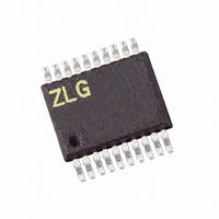
IC ENCORE MCU FLASH 4K 20SSOP
Manufacturer
Zilog
Series
Encore!® XP®r
Specifications of Z8F0411HH020SG
Core Processor
Z8
Core Size
8-Bit
Speed
20MHz
Connectivity
I²C, IrDA, UART/USART
Peripherals
Brown-out Detect/Reset, POR, PWM, WDT
Number Of I /o
11
Program Memory Size
4KB (4K x 8)
Program Memory Type
FLASH
Ram Size
1K x 8
Voltage - Supply (vcc/vdd)
2.7 V ~ 3.6 V
Oscillator Type
Internal
Operating Temperature
0°C ~ 70°C
Package / Case
20-SSOP
Controller Family/series
Z8
No. Of I/o's
11
Ram Memory Size
1KB
Cpu Speed
20MHz
No. Of Timers
2
Rohs Compliant
Yes
Processor Series
Z8F041xx
Core
eZ8
Data Bus Width
8 bit
Data Ram Size
1 KB
Interface Type
I2C, UART
Maximum Clock Frequency
20 MHz
Number Of Programmable I/os
11
Number Of Timers
2
Operating Supply Voltage
2.7 V to 3.6 V
Maximum Operating Temperature
+ 70 C
Mounting Style
SMD/SMT
Minimum Operating Temperature
0 C
For Use With
770-1002 - ISP 4PORT ZILOG Z8 ENCORE! MCU269-4643 - KIT DEV Z8 ENCORE XP 28-PIN269-4630 - DEV KIT FOR Z8 ENCORE 8K/4K269-4629 - KIT DEV Z8 ENCORE XP 28-PIN269-4628 - KIT DEV Z8 ENCORE XP 8-PIN
Lead Free Status / RoHS Status
Lead free / RoHS Compliant
Eeprom Size
-
Data Converters
-
Lead Free Status / Rohs Status
Details
Other names
269-4101
Z8F0411HH020SG
Z8F0411HH020SG
Available stocks
Company
Part Number
Manufacturer
Quantity
Price
Company:

Part Number:
Z8F0411HH020SG
Manufacturer:
Zilog
Quantity:
68


Table 15. Port A–C Control Registers (PxCTL)
Table 16. Port A–C Data Direction Sub-Registers
PS022517-0508
BITS
FIELD
RESET
R/W
ADDR
BITS
FIELD
RESET
R/W
ADDR
Port A–C Control Registers
7
7
DD7
If 01H in Port A–C Address Register, accessible through the Port A–C Control Register
The Port A–C Control Registers set the GPIO port operation. The value in the correspond-
ing Port A–C Address Register determines the control sub-registers accessible using the
Port A–C Control Register
PCTL[7:0]—Port Control
The Port Control Register provides access to all sub-registers that configure the GPIO Port
operation.
Port A–C Data Direction Sub-Registers
The Port A–C Data Direction sub-register is accessed through the Port A–C Control
register by writing 01H to the Port A–C Address Register
DD[7:0]—Data Direction
These bits control the direction of the associated port pin. Port Alternate Function
operation overrides the Data Direction register setting.
0 = Output. Data in the Port A–C Output Data Register is driven onto the port pin.
1 = Input. The port pin is sampled and the value written into the Port A–C Input
Port A–C Alternate Function Sub-Registers
The Port A–C Alternate Function sub-register
Port A–C Control Register by writing
Port A–C Alternate Function sub-registers select the alternate functions for the selected
Data Register. The output driver is tri-stated.
6
6
DD6
5
5
DD5
(Table
4
4
FD1H, FD5H, FD9H
DD4
15).
02H
PCTL
R/W
R/W
00H
1
3
3
to the Port A–C Address Register. The
DD3
(Table
17) is accessed through the
2
2
Z8 Encore! XP
DD2
(Table
General-Purpose Input/Output
Product Specification
16).
1
1
DD1
®
F0822 Series
0
0
DD0
51
Related parts for Z8F0411HH020SG
Image
Part Number
Description
Manufacturer
Datasheet
Request
R

Part Number:
Description:
Communication Controllers, ZILOG INTELLIGENT PERIPHERAL CONTROLLER (ZIP)
Manufacturer:
Zilog, Inc.
Datasheet:

Part Number:
Description:
KIT DEV FOR Z8 ENCORE 16K TO 64K
Manufacturer:
Zilog
Datasheet:

Part Number:
Description:
KIT DEV Z8 ENCORE XP 28-PIN
Manufacturer:
Zilog
Datasheet:

Part Number:
Description:
DEV KIT FOR Z8 ENCORE 8K/4K
Manufacturer:
Zilog
Datasheet:

Part Number:
Description:
KIT DEV Z8 ENCORE XP 28-PIN
Manufacturer:
Zilog
Datasheet:

Part Number:
Description:
DEV KIT FOR Z8 ENCORE 4K TO 8K
Manufacturer:
Zilog
Datasheet:
Part Number:
Description:
CMOS Z8 microcontroller. ROM 16 Kbytes, RAM 256 bytes, speed 16 MHz, 32 lines I/O, 3.0V to 5.5V
Manufacturer:
Zilog, Inc.
Datasheet:
Part Number:
Description:
Low-cost microcontroller. 512 bytes ROM, 61 bytes RAM, 8 MHz
Manufacturer:
Zilog, Inc.
Datasheet:
Part Number:
Description:
Z8 4K OTP Microcontroller
Manufacturer:
Zilog, Inc.
Datasheet:
Part Number:
Description:
CMOS SUPER8 ROMLESS MCU
Manufacturer:
Zilog, Inc.
Datasheet:
Part Number:
Description:
SL1866 CMOSZ8 OTP Microcontroller
Manufacturer:
Zilog, Inc.
Datasheet:
Part Number:
Description:
SL1866 CMOSZ8 OTP Microcontroller
Manufacturer:
Zilog, Inc.
Datasheet:
Part Number:
Description:
OTP (KB) = 1, RAM = 125, Speed = 12, I/O = 14, 8-bit Timers = 2, Comm Interfaces Other Features = Por, LV Protect, Voltage = 4.5-5.5V
Manufacturer:
Zilog, Inc.
Datasheet:
Part Number:
Description:
Manufacturer:
Zilog, Inc.
Datasheet: