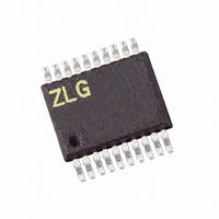
Z8F0411HH020SG Zilog, Z8F0411HH020SG Datasheet - Page 130

Z8F0411HH020SG
Manufacturer Part Number
Z8F0411HH020SG
Description
IC ENCORE MCU FLASH 4K 20SSOP
Manufacturer
Zilog
Series
Encore!® XP®r
Specifications of Z8F0411HH020SG
Core Processor
Z8
Core Size
8-Bit
Speed
20MHz
Connectivity
I²C, IrDA, UART/USART
Peripherals
Brown-out Detect/Reset, POR, PWM, WDT
Number Of I /o
11
Program Memory Size
4KB (4K x 8)
Program Memory Type
FLASH
Ram Size
1K x 8
Voltage - Supply (vcc/vdd)
2.7 V ~ 3.6 V
Oscillator Type
Internal
Operating Temperature
0°C ~ 70°C
Package / Case
20-SSOP
Controller Family/series
Z8
No. Of I/o's
11
Ram Memory Size
1KB
Cpu Speed
20MHz
No. Of Timers
2
Rohs Compliant
Yes
Processor Series
Z8F041xx
Core
eZ8
Data Bus Width
8 bit
Data Ram Size
1 KB
Interface Type
I2C, UART
Maximum Clock Frequency
20 MHz
Number Of Programmable I/os
11
Number Of Timers
2
Operating Supply Voltage
2.7 V to 3.6 V
Maximum Operating Temperature
+ 70 C
Mounting Style
SMD/SMT
Minimum Operating Temperature
0 C
For Use With
770-1002 - ISP 4PORT ZILOG Z8 ENCORE! MCU269-4643 - KIT DEV Z8 ENCORE XP 28-PIN269-4630 - DEV KIT FOR Z8 ENCORE 8K/4K269-4629 - KIT DEV Z8 ENCORE XP 28-PIN269-4628 - KIT DEV Z8 ENCORE XP 8-PIN
Lead Free Status / RoHS Status
Lead free / RoHS Compliant
Eeprom Size
-
Data Converters
-
Lead Free Status / Rohs Status
Details
Other names
269-4101
Z8F0411HH020SG
Z8F0411HH020SG
Available stocks
Company
Part Number
Manufacturer
Quantity
Price
Company:
Part Number:
Z8F0411HH020SG
Manufacturer:
Zilog
Quantity:
68
- Current page: 130 of 264
- Download datasheet (6Mb)
PS022517-0508
Input Sample Time
(CLKPOL = 0)
(CLKPOL = 1)
Transfer Format PHASE is 0
Figure 23
to 0. The two SCK waveforms show polarity with CLKPOL reset to 0 and with CLKPOL
set to one. The diagram can be interpreted as either a Master or Slave timing diagram since
the SCK Master-In/Slave-Out (MISO) and Master-Out/Slave-In (MOSI) pins are directly
connected between the Master and the Slave.
Transfer Format PHASE is 1
Figure 24
waveforms are depicted for SCK, one for CLKPOL reset to 0 and another for CLKPOL
set to 1.
MOSI
MISO
SCK
SCK
SS
displays the timing diagram for an SPI transfer in which PHASE is cleared
displays the timing diagram for an SPI transfer in which PHASE is one. Two
Bit7
Bit7
Figure 23. SPI Timing When PHASE is 0
Bit6
Bit6
Bit5
Bit5
Bit4
Bit4
Bit3
Bit3
Bit2
Bit2
Z8 Encore! XP
Bit1
Bit1
Product Specification
Serial Peripheral Interface
Bit0
Bit0
®
F0822 Series
117
Related parts for Z8F0411HH020SG
Image
Part Number
Description
Manufacturer
Datasheet
Request
R

Part Number:
Description:
Communication Controllers, ZILOG INTELLIGENT PERIPHERAL CONTROLLER (ZIP)
Manufacturer:
Zilog, Inc.
Datasheet:

Part Number:
Description:
KIT DEV FOR Z8 ENCORE 16K TO 64K
Manufacturer:
Zilog
Datasheet:

Part Number:
Description:
KIT DEV Z8 ENCORE XP 28-PIN
Manufacturer:
Zilog
Datasheet:

Part Number:
Description:
DEV KIT FOR Z8 ENCORE 8K/4K
Manufacturer:
Zilog
Datasheet:

Part Number:
Description:
KIT DEV Z8 ENCORE XP 28-PIN
Manufacturer:
Zilog
Datasheet:

Part Number:
Description:
DEV KIT FOR Z8 ENCORE 4K TO 8K
Manufacturer:
Zilog
Datasheet:

Part Number:
Description:
CMOS Z8 microcontroller. ROM 16 Kbytes, RAM 256 bytes, speed 16 MHz, 32 lines I/O, 3.0V to 5.5V
Manufacturer:
Zilog, Inc.
Datasheet:

Part Number:
Description:
Low-cost microcontroller. 512 bytes ROM, 61 bytes RAM, 8 MHz
Manufacturer:
Zilog, Inc.
Datasheet:

Part Number:
Description:
Z8 4K OTP Microcontroller
Manufacturer:
Zilog, Inc.
Datasheet:

Part Number:
Description:
CMOS SUPER8 ROMLESS MCU
Manufacturer:
Zilog, Inc.
Datasheet:

Part Number:
Description:
SL1866 CMOSZ8 OTP Microcontroller
Manufacturer:
Zilog, Inc.
Datasheet:

Part Number:
Description:
SL1866 CMOSZ8 OTP Microcontroller
Manufacturer:
Zilog, Inc.
Datasheet:

Part Number:
Description:
OTP (KB) = 1, RAM = 125, Speed = 12, I/O = 14, 8-bit Timers = 2, Comm Interfaces Other Features = Por, LV Protect, Voltage = 4.5-5.5V
Manufacturer:
Zilog, Inc.
Datasheet:

Part Number:
Description:
Manufacturer:
Zilog, Inc.
Datasheet:


