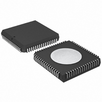
PXAS37KBA,512 NXP Semiconductors, PXAS37KBA,512 Datasheet - Page 40

PXAS37KBA,512
Manufacturer Part Number
PXAS37KBA,512
Description
IC XA MCU 16BIT 32K OTP 68-PLCC
Manufacturer
NXP Semiconductors
Series
XAr
Datasheet
1.PXAS30KBA512.pdf
(52 pages)
Specifications of PXAS37KBA,512
Core Processor
XA
Core Size
16-Bit
Speed
30MHz
Connectivity
EBI/EMI, I²C, UART/USART
Peripherals
PWM, WDT
Number Of I /o
50
Program Memory Size
32KB (32K x 8)
Program Memory Type
OTP
Ram Size
1K x 8
Voltage - Supply (vcc/vdd)
2.7 V ~ 5.5 V
Data Converters
A/D 8x8b
Oscillator Type
External
Operating Temperature
0°C ~ 70°C
Package / Case
68-PLCC
Processor Series
PXAS3x
Core
80C51
Data Bus Width
16 bit
Data Ram Size
1 KB
Interface Type
I2C, UART
Maximum Clock Frequency
30 MHz
Number Of Programmable I/os
50
Number Of Timers
3
Operating Supply Voltage
2.7 V to 5.5 V
Maximum Operating Temperature
+ 70 C
Mounting Style
SMD/SMT
Minimum Operating Temperature
0 C
On-chip Adc
8 bit, 8 Channel
Lead Free Status / RoHS Status
Lead free / RoHS Compliant
Eeprom Size
-
Lead Free Status / Rohs Status
Details
Other names
568-3536-5
935262377512
PXAS37KBA
935262377512
PXAS37KBA
Available stocks
Company
Part Number
Manufacturer
Quantity
Price
Company:
Part Number:
PXAS37KBA,512
Manufacturer:
TI
Quantity:
5
Company:
Part Number:
PXAS37KBA,512
Manufacturer:
NXP Semiconductors
Quantity:
10 000
Philips Semiconductors
AC ELECTRICAL CHARACTERISTICS (3 V)
V
NOTES ON PAGE 41.
2000 Dec 01
Address Cycle
Code Read Cycle
Data Read Cycle
Data Write Cycle
Wait Input
DD
SYMBOL
SYMBOL
XA 16-bit microcontroller
32 K/1 K OTP/ROM/ROMless, 8-channel 8-bit A/D, low voltage (2.7 V–5.5 V),
I
t
t
t
t
t
t
t
t
t
t
t
t
t
t
t
t
t
t
t
t
t
t
t
t
t
t
t
LHLL
AVLL
LLAX
PLPH
LLPL
AVIVA
AVIVB
PLIV
PHIX
PHIZ
IXUA
RLRH
LLRL
AVDVA
AVDVB
RLDV
RHDX
RHDZ
DXUA
WLWH
LLWL
QVWX
WHQX
AVWL
UAWH
WTH
WTL
2
C, 2 UARTs, 16 MB address range
= 2.7 V to 4.5 V; T
26, 28, 30
26, 28, 30
26, 28, 30
FIGURE
FIGURE
26
26
26
27
26
26
26
26
28
28
28
29
28
28
28
28
30
30
30
30
30
30
31
31
amb
= 0 to +70 C for commercial, T
ALE pulse width (programmable)
Address valid to ALE de-asserted (set-up)
Address hold after ALE de-asserted
PSEN pulse width
ALE de-asserted to PSEN asserted
Address valid to instruction valid, ALE cycle (access time)
Address valid to instruction valid, non-ALE cycle (access time)
PSEN asserted to instruction valid (enable time)
Instruction hold after PSEN de-asserted
Bus 3-State after PSEN de-asserted
Hold time of unlatched part of address after instruction latched
RD pulse width
ALE de-asserted to RD asserted
Address valid to data input valid, ALE cycle (access time)
Address valid to data input valid, non-ALE cycle (access time)
RD low to valid data in (enable time)
Data hold time after RD de–asserted
Bus 3-State after RD de-asserted (disable time)
Hold time of unlatched part of address after data latched
WR pulse width
ALE falling edge to WR asserted
Data valid before WR asserted (data set-up time)
Data hold time after WR de-asserted (Note 6)
Address valid to WR asserted (address set-up time) (Note 5)
Hold time of unlatched part of address after WR is de-asserted
WAIT stable after bus strobe (RD, WR, or PSEN) asserted
WAIT hold after bus strobe (RD, WR, or PSEN) asserted
PARAMETER
PARAMETER
amb
= –40 C to +85 C for industrial.
40
(V12 * t
(V13 * t
(V11 * t
(V1 * t
(V1 * t
(V2 * t
(V7 * t
(V8 * t
(V11 * t
(V9 * t
(V10 * t
(t
(t
(t
C
C
C
/2) – 12
MIN
/2) – 9
/2) – 9
0
0
0
0
C
C
C
C
C
C
C
C
C
) – 10
) – 18
) – 12
) – 12
) – 12
C
) – 28
C
) – 10
) – 10
) – 28
) – 8
) – 5
LIMITS
(V10 * t
(V3 * t
(V4 * t
(V2 * t
(V6 * t
(V5 * t
(V7 * t
t
t
MAX
C
C
Preliminary specification
C
C
C
C
C
C
– 8
– 8
C
) – 58
) – 52
) – 52
) – 58
) – 52
) – 52
) – 40
XA-S3
UNIT
UNIT
ns
ns
ns
ns
ns
ns
ns
ns
ns
ns
ns
ns
ns
ns
ns
ns
ns
ns
ns
ns
ns
ns
ns
ns
ns
ns
ns


