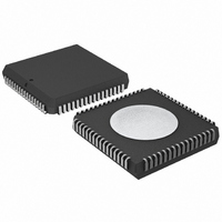
PXAS37KBA,512 NXP Semiconductors, PXAS37KBA,512 Datasheet - Page 36

PXAS37KBA,512
Manufacturer Part Number
PXAS37KBA,512
Description
IC XA MCU 16BIT 32K OTP 68-PLCC
Manufacturer
NXP Semiconductors
Series
XAr
Datasheet
1.PXAS30KBA512.pdf
(52 pages)
Specifications of PXAS37KBA,512
Core Processor
XA
Core Size
16-Bit
Speed
30MHz
Connectivity
EBI/EMI, I²C, UART/USART
Peripherals
PWM, WDT
Number Of I /o
50
Program Memory Size
32KB (32K x 8)
Program Memory Type
OTP
Ram Size
1K x 8
Voltage - Supply (vcc/vdd)
2.7 V ~ 5.5 V
Data Converters
A/D 8x8b
Oscillator Type
External
Operating Temperature
0°C ~ 70°C
Package / Case
68-PLCC
Processor Series
PXAS3x
Core
80C51
Data Bus Width
16 bit
Data Ram Size
1 KB
Interface Type
I2C, UART
Maximum Clock Frequency
30 MHz
Number Of Programmable I/os
50
Number Of Timers
3
Operating Supply Voltage
2.7 V to 5.5 V
Maximum Operating Temperature
+ 70 C
Mounting Style
SMD/SMT
Minimum Operating Temperature
0 C
On-chip Adc
8 bit, 8 Channel
Lead Free Status / RoHS Status
Lead free / RoHS Compliant
Eeprom Size
-
Lead Free Status / Rohs Status
Details
Other names
568-3536-5
935262377512
PXAS37KBA
935262377512
PXAS37KBA
Available stocks
Company
Part Number
Manufacturer
Quantity
Price
Company:
Part Number:
PXAS37KBA,512
Manufacturer:
TI
Quantity:
5
Company:
Part Number:
PXAS37KBA,512
Manufacturer:
NXP Semiconductors
Quantity:
10 000
1. Conditions: AV
2. The differential non-linearity (DL
3. The ADC is monotonic, there are no missing codes.
4. The integral non-linearity (IL
5. The offset error (OS
6. The gain error (G
7. The absolute voltage error (A
8. This should be considered when both analog and digital signals are input simultaneously to Port 5. Parameter is guaranteed by design.
9. 10-bit mode only.
10. 10-bit mode is only operational up to f
Philips Semiconductors
10-BIT
T
NOTES:
2000 Dec 01
amb
AV
AI
AI
AI
AV
R
C
DL
IL
OS
G
A
M
C
SYMBOL
SYMBOL
XA 16-bit microcontroller
32 K/1 K OTP/ROM/ROMless, 8-channel 8-bit A/D, low voltage (2.7 V–5.5 V),
I
REF
IA
e
t
appropriate adjustment of gain and offset errors. See Figure 25.
the straight line which fits the ideal transfer curve. See Figure 25.
and the straight line which fits the ideal transfer curve. Gain error is constant at every point on the transfer curve. See Figure 25.
ADC and the ideal transfer curve.
2
e
e
CTC
DD
ID
PD
DD
IN
e
C, 2 UARTs, 16 MB address range
e
= 0 to +70 C for commercial, T
10
MODE A/D CONVERTER DC ELECTRICAL CHARACTERISTICS
Analog supply voltage
Analog supply current (operating)
Analog supply current (Idle mode)
Analog supply current (Power-Down mode)
Analog input voltage
Resistance between V
Analog input capacitance
Differential non-linearity
Integral non-linearity
Offset error
Gain error
Absolute voltage error (with averaging)
Channel-to-channel matching
Crosstalk between inputs of port
REF–
e
) is the relative difference in percent between the straight line fitting the actual transfer curve (after removing offset error),
e
= 0 V; AV
) is the absolute difference between the straight line which fits the actual transfer curve (after removing gain error), and
1, 6
1, 5
PARAMETER
PARAMETER
e
) is the peak difference between the center of the steps of the actual and the ideal transfer curve after
e
REF+
) is the maximum difference between the center of the steps of the actual transfer curve of the non-calibrated
e
1, 4
amb
) is the difference between the actual step width and the ideal step width. See Figure 25.
REF+
= 3.07 V.
1, 2, 3
= –40 to +85 C for industrial, unless otherwise specified.
C
= 20 MHz.
and V
8
REF–
1, 7
Commercial temperature range
Industrial temperature range
TEST CONDITIONS
TEST CONDITIONS
Port 5 = 0 to AV
0 – 100 kHz
36
DD
AV
SS
MIN
125
2.7
–0.2
LIMITS
AV
MAX
DD
100
150
225
–60
2.5
3.3
2.5
2.5
15
1
6
1
8
Preliminary specification
1
+0.2
9
9
9
9
9
XA-S3
UNIT
UNIT
LSB
LSB
LSB
LSB
LSB
mA
k
pF
dB
%
V
V
A
A
A


