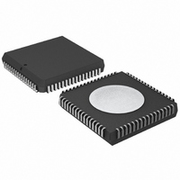
P87C554SFAA,512 NXP Semiconductors, P87C554SFAA,512 Datasheet - Page 33

P87C554SFAA,512
Manufacturer Part Number
P87C554SFAA,512
Description
IC 80C51 MCU 16K OTP 64-PLCC
Manufacturer
NXP Semiconductors
Series
87Cr
Specifications of P87C554SFAA,512
Core Processor
8051
Core Size
8-Bit
Speed
16MHz
Connectivity
EBI/EMI, I²C, UART/USART
Peripherals
POR, PWM, WDT
Number Of I /o
40
Program Memory Size
16KB (16K x 8)
Program Memory Type
OTP
Ram Size
512 x 8
Voltage - Supply (vcc/vdd)
2.7 V ~ 5.5 V
Data Converters
A/D 8x10b
Oscillator Type
Internal
Operating Temperature
-40°C ~ 85°C
Package / Case
68-PLCC
Cpu Family
87C
Device Core
80C51
Device Core Size
8b
Frequency (max)
16MHz
Interface Type
I2C/UART
Total Internal Ram Size
512Byte
# I/os (max)
40
Number Of Timers - General Purpose
3
Operating Supply Voltage (typ)
5V
Operating Supply Voltage (max)
5.5V
Operating Supply Voltage (min)
4.5V
On-chip Adc
7-chx10-bit
Instruction Set Architecture
CISC
Operating Temp Range
-40C to 85C
Operating Temperature Classification
Industrial
Mounting
Surface Mount
Pin Count
68
Package Type
PLCC
Processor Series
P87C5x
Core
80C51
Data Bus Width
8 bit
Data Ram Size
512 B
Maximum Clock Frequency
16 MHz
Number Of Programmable I/os
40
Number Of Timers
3
Operating Supply Voltage
2.7 V to 5.5 V
Maximum Operating Temperature
+ 85 C
Mounting Style
SMD/SMT
3rd Party Development Tools
PK51, CA51, A51, ULINK2
Minimum Operating Temperature
- 40 C
Package
68PLCC
Family Name
87C
Maximum Speed
16 MHz
Lead Free Status / RoHS Status
Lead free / RoHS Compliant
Eeprom Size
-
Lead Free Status / Rohs Status
Compliant
Other names
568-1255-5
935263922512
P87C554SFAA
935263922512
P87C554SFAA
Available stocks
Company
Part Number
Manufacturer
Quantity
Price
Company:
Part Number:
P87C554SFAA,512
Manufacturer:
Maxim
Quantity:
145
Company:
Part Number:
P87C554SFAA,512
Manufacturer:
NXP Semiconductors
Quantity:
10 000
Philips Semiconductors
SIO1 Implementation and Operation: Figure 35 shows how the
on-chip I
describes the individual blocks.
I
The input filters have I
is less than 1.5 V, the input logic level is interpreted as 0; if the input
voltage is greater than 3.0 V, the input logic level is interpreted as 1.
Input signals are synchronized with the internal clock (f
spikes shorter than three oscillator periods are filtered out.
The output stages consist of open drain transistors that can sink
3 mA at V
clamping diodes to V
bus and V
A
This 8-bit special function register may be loaded with the 7-bit slave
address (7 most significant bits) to which SIO1 will respond when
programmed as a slave transmitter or receiver. The LSB (GC) is
used to enable general call address (00H) recognition.
2003 Jan 28
NPUT
DDRESS
SDA
SCL
80C51 8-bit microcontroller – 6-clock operation
16K/512 OTP/ROMless, 7 channel 10 bit A/D, I
high I/O, 64L LQFP
CONDITION
F
ILTERS AND
START
2
R
C bus interface is implemented, and the following text
OUT
S
DD
EGISTER,
is switched off, the I
< 0.4 V. These open drain outputs do not have
I
2
C bus
MSB
O
S
UTPUT
1
DD
1
2
ADR
C compatible input levels. If the input voltage
. Thus, if the device is connected to the I
SLAVE ADDRESS
S
TAGES
2
P1.7/SDA
2
C bus is not affected.
8XC554
P1.6/SCL
7
Figure 33. Typical I
DIRECTION
Figure 34. Data Transfer on the I
SIGNAL FROM RECEIVER
ACKNOWLEDGMENT
R/W
BIT
8
OSC
/2), and
OTHER DEVICE WITH
ACK
9
I
2
R
2
C
P
C INTERFACE
2
C, PWM, capture/compare,
33
2
C Bus Configuration
R
C
The comparator compares the received 7-bit slave address with its
own slave address (7 most significant bits in S1ADR). It also
compares the first received 8-bit byte with the general call address
(00H). If an equality is found, the appropriate status bits are set and
an interrupt is requested.
S
This 8-bit special function register contains a byte of serial data to
be transmitted or a byte which has just been received. Data in
S1DAT is always shifted from right to left; the first bit to be
transmitted is the MSB (bit 7) and, after a byte has been received,
the first bit of received data is located at the MSB of S1DAT. While
data is being shifted out, data on the bus is simultaneously being
shifted in; S1DAT always contains the last byte present on the bus.
Thus, in the event of lost arbitration, the transition from master
transmitter to slave receiver is made with the correct data in S1DAT.
P
HIFT
OMPARATOR
V
1
CLOCK LINE HELD LOW WHILE
INTERRUPTS ARE SERVICED
DD
R
EGISTER,
REPEATED IF MORE BYTES
ARE TRANSFERRED
2
C Bus
2
S
OTHER DEVICE WITH
1
DAT
SIGNAL FROM RECEIVER
I
2
3–8
C INTERFACE
ACKNOWLEDGMENT
ACK
9
SU00964
80C554/87C554
SDA
SCL
P/S
Product data
CONDITION
CONDITION
REPEATED
SU00965
START
STOP


